Highlights
Manipulating Crystal Orientation in Nanopores
Marc Hillmyer
Magnetics Day - Magnetism in Technology
Paul Crowell, Chris Leighton, Dan Dahlberg
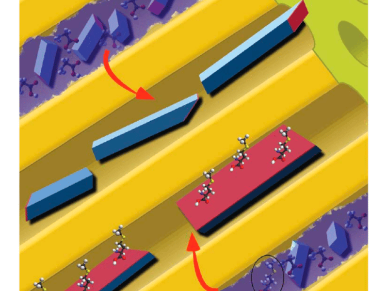
Defect Density Limits Orientational Order in Shear-Aligned Block Copolymer Films
Andy Marencic, Mingshaw Wu, Paul Chaikin (NYU), and Rick Register
Multiscale Patterning of Plasmonic Metamaterials
Joel Henzie, Min Hyung Lee, and Teri W. Odom Northwestern University Materials Research Science & Engineering Center, DMR-0520513
Atomic Force Photovoltaic Microscopy
B. J. Leever, M. F. Durstock, M. D. Irwin, A. W. Hains, T. J. Marks, L. S. C. Pingree, and M. C. Hersam Northwestern University Materials Research Science & Engineering Center DMR-0520513
The Art of Science and the Science of Art
Katherine T. Faber Northwestern University Materials Research Science & Engineering Center, DMR-0520513
Quantum Memory Preserves Coherence for over 1 Second in Silicon
John J. L. Morton, Alexei M. Tyryshkin, Richard M. Brown, Shyam Shankar, Brendon W. Lovett, Arzhang Ardavan, Thomas Schenkel, Eugene E. Haller, Joel W. Ager and Stephen A. Lyon
Showing 1251 to 1260 of 1452