While many approaches have been developed over the years to transfer patterns onto flat surfaces, faithfully transferring patterns onto curves substrates remains a major obstacle to the development of large-area electronics. Recently, PCCM researchers have successfully patterned domed polyester substrates with metal stripes (gold, silver, etc.). They employed a soft, pre-patterned elastomeric stamp coated with a thin layer of metal by electron-beam evaporation, bent into a complementary hemisphere. By coating the polyester dome with a thin metal strike layer and bringing the two into contact, cold welding occurs, successfully transferring the gold or silver stripes. This demonstration significantly extends the ability of direct transfer patterning, previously only demonstrated on planar substrates, to advanced optical and electronic applications. In particular, this technique was applied to produce a passive, organic focal plane array directly onto a transparent polyester hemisphere.
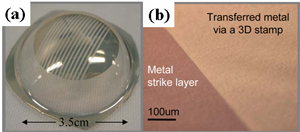
(a) Optical microscope image of the Au stripes (500 Â’µm feature size) patterned on a dome via a 3D elastomeric (PDMS) stamp. (b) No fracture observed in metal stripe transferred from stamp.