Highlights
Apr 28, 2021
Big Idea: Quantum Leap
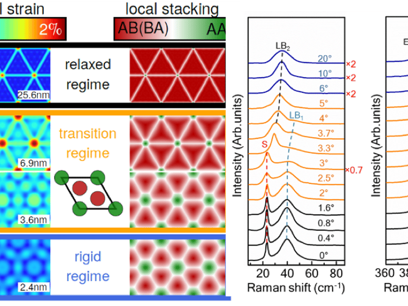
Collective Excitations in Twisted Bilayers
X. Li, A. MacDonald, K. Lai, C. K. Shih: Univ. of Texas at Austin
Moire superlattices consist of two monolayers of atomically thin materials, in this case the transition metal dichalcogenide MoS2, stacked on top of each other with a slight rotational misalignment (twist) that creates a moire interference pattern between the atomic lattices of the two monolayers.
Apr 6, 2021
University of California, Santa Barbara
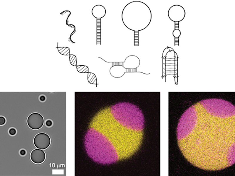
Seed: Selecting for Phase-Separating Nucleic Acid Coacervates
Top: Designed DNA structures of varying charge density and flexibility. Bottom left: Coacervate droplets formed from 1 DNA structure. Bottom middle/right: Binary droplets formed from a model system with 2 DNA structures.
Apr 6, 2021
University of California, Santa Barbara
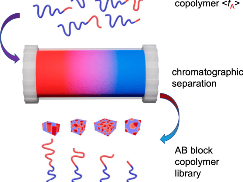
IRG-3: Accelerating Block Copolymer Research
A single parent diblock copolymer can be purified by automated chromatography to give libraries of well-defined, low dispersity block copolymers on multi-gram scale.
Apr 6, 2021
University of California, Santa Barbara
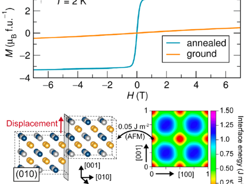
IRG-1: Magnetoplastic Coupling in Heusler Intermetallics
Experiments (top) showing near zero-net magnetization of MnAu2Al following plastic deformation and simulations (bottom) of low energy displacive pathways enabled by local spin orderings.
Apr 6, 2021
University of California, Santa Barbara
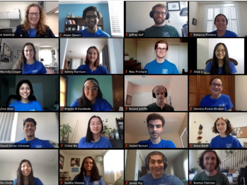
UC Santa Barbara MRSEC Continues REU Program Through COVID-19 Lockdown
The UC Santa Barbara ran a fully remote REU program in Summer 2020, with 18 students working on primarily computational projects.
18 students participated from 8 different colleges and universities. In addition to research, students participated in weekly intern group meetings, and weekly Zoom career building workshops, including Tips on Talks, Figures for Presentations, Poster Making, Finding Positions in Industry, Graduate School Panel, and others. All students presented their results in a virtual Summer Intern Colloquium.
Mar 4, 2021
Big Idea: Future of Work at the Human-Technology Frontier, Materials Under Extreme Conditions
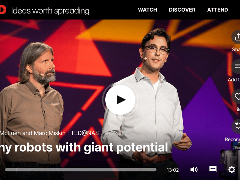
Tiny Robots with Giant Potential (TED Talk)
Take a trip down the microworld as roboticists Paul McEuen and Marc Miskin explain how they design and mass-produce microrobots the size of a single cell, powered by atomically thin legs -- and show how these machines could one day be "piloted" to battle crop diseases or study your brain at the level of individual neurons.
Jun 13, 2020
Big Idea: Growing Convergence Research
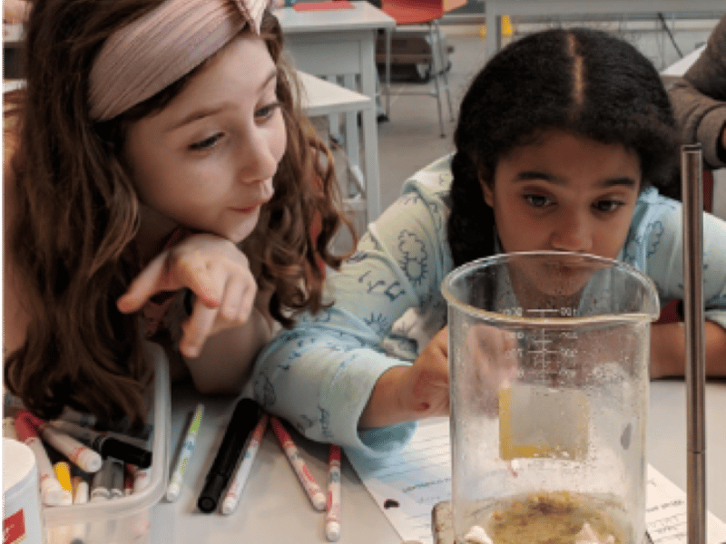
NYU-MRSEC & BioBus Collaboration
Scientific Frontiers Program, New York University & BioBus
NYU-MRSEC investigators have worked alongside BioBus scientists to develop new K-12 materials science-related curricula since 2009. This collaboration brought exciting and educational engineering projects to over 1,000 NYC students in 2019-2020.
Jun 12, 2020
Big Idea: Future of Work at the Human-Technology Frontier
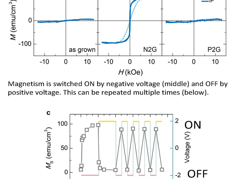
Voltage Control of Magnetism above Room Temperature in epitaxial SrCo1-xFexO3-δ
Caroline A. Ross
Searching for new materials and phenomena to enable voltage control of magnetism and magnetic properties holds compelling interest for the development of low-power non-volatile memory devices. Here, we report on a non-volatile ON/OFF voltage control of magnetism in thin films of an oxide, SrCo1-xFexO3-δ (SCFO).
Jun 12, 2020
Big Idea: Understanding the Rules of Life
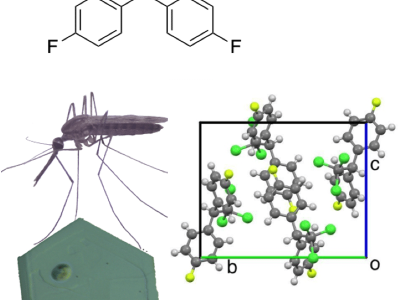
Manipulating Solid Forms of Contact Insecticides for Infectious Disease Prevention
X. Zhu, C. T. Hu, J. Yang, L. A. Joyce, M. Qiu, M. D. Ward, B. Kahr
MRSEC investigators rediscovered DFDT and found that amorphous and crystalline forms of DFDT and a mono-fluorinated chiral congener, MFDT were more active against Anopheles and Aedes mosquitoes, the former the disease vector for malaria and the latter for Zika, yellow fever, dengue, and chikungunya.
Jun 12, 2020
New York University
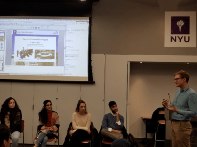
Path to the PhD Panel Discussion
NYU MRSEC & NYU CSTEP
NYU-MRSEC pursues its partnership with NYU-CSTEP (Collegiate Science and Technology Entry Program). The Center was invited to give a guest lecture as part of the NYU-CSTEP Research Initiative.
Showing 301 to 310 of 1452