Highlights
Bioinspired 3D-Printed Hydrogel Actuators that Perspire
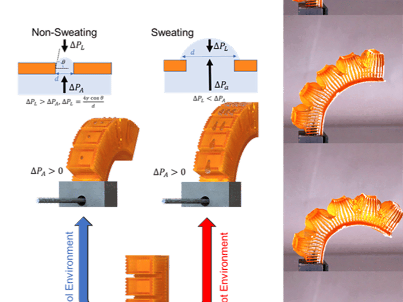
This project has developed finger-like 3D printed hydrogel actuators with autonomic perspiratioon, as shown in the top left image. Actuation is created by using a Polyacrylamide-based dorsal layer, and a Poly(N-isopropylacrylamide) finger. when the finger bends, In the figures at bottom left, when body temperature is below 30 degrees C, 'skin' pores are closed and allow for mechanical actuation. When temperature rises above 30 degrees C, skin pores open, allowing localized perspiration and actuation simultaneously. A. Mishra, W. Pan, E. P. Giannelis, R. F. Shepherd, T. J. Wallin. Cornell University
Partnerships for Commercializing New Technologies
Solid-Phase Epitaxy: A Means to Control Atomic-Scale Structure in Complex Materials
New Insights into Surface Diffusion on Glasses
Lian Yu, Dane Morgan, John Perepezko, Paul Voyles, Mark Ediger, University of Wisconsin-Madison
Accelerating Innovation through Licensing, Commercialization, and Startups
Knowledge Transfer, Northwestern University MRSEC
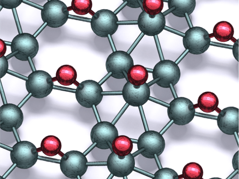
Synthesis of Borophane Polymorphs through Hydrogenation of Borophene
Q. Li, V. S. C. Kolluru, M. S. Rahn, E. Schwenker, S. Li, R. G. Hennig, P. Darancet, M. K. Y. Chan, and M. C. Hersam, “Synthesis of borophane polymorphs through hydrogenation of borophene,” Science, 371, 1143-1148 (2021).

STEM: Science and Beyond
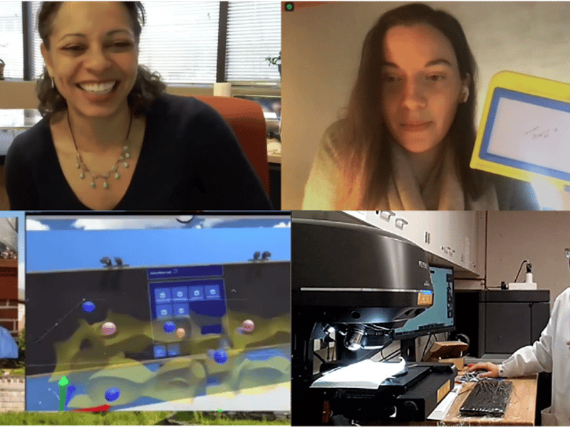
Virtual Musical Magnetism Engages Middle School Students in Materials Science
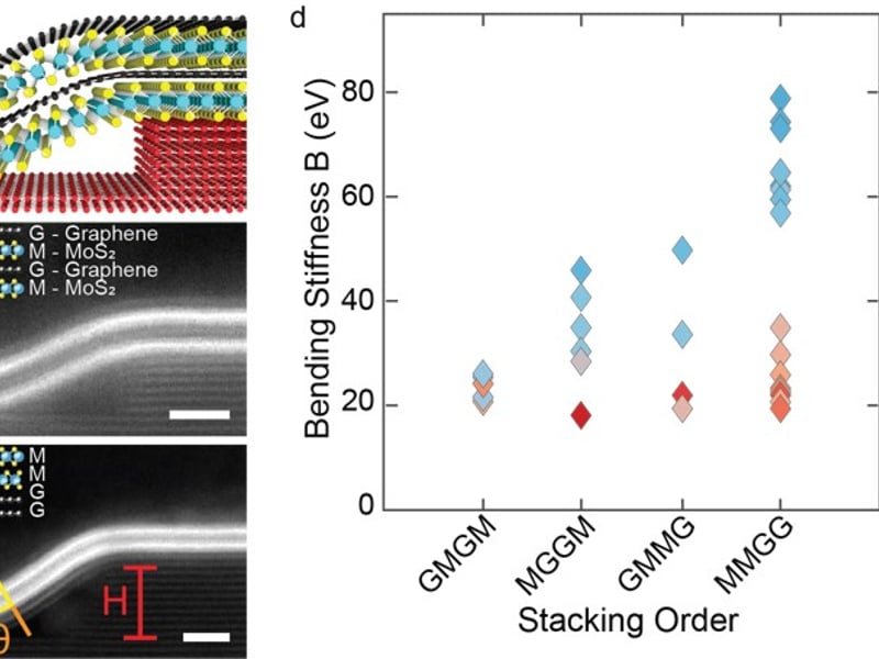
Designing Highly Deformable 2D Materials and Heterostructures
A. M. van der Zande, P. Y. Huang, and E. Ertekin, University of Illinois at Urbana-Champaign
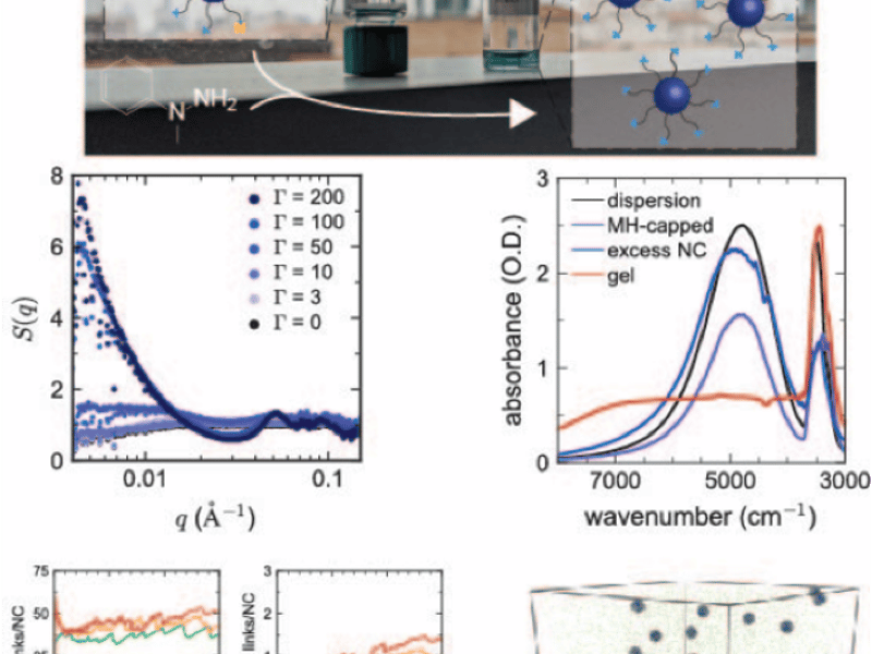
Assembly of Linked Nanocrystal Colloids by Reversible Covalent Bonds
D. Milliron, E. Anslyn, T. Truskett: Univ. of Texas at Austin
Showing 291 to 300 of 1452