Highlights
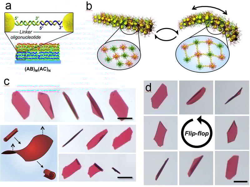
SEED Team Builds Simple Microrobots from DNA
T.S. Shim, D. Chenoweth (Chemistry), D. Lee (Chemical and Biomolecular Engineering), S.J. Park (Chemistry), J.C. Crocker (Chemical and Biomolecular Engineering) Dr. Tae Soup Shim (left) & Dr. Mehdi Zanjani (right)
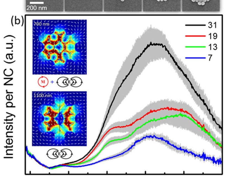
Probing the Evolution of Plasmonic Properties in Nanocrystal Oligomer Metamolecules
N.J. Greybush, I. Liberal, L. Malassis, J.M. Kikkawa (Physics), N. Engheta (Electrical and Systems Engineering), C.B. Murray (Chemistry), C.R. Kagan (Electrical and Systems Engineering) MRSEC student Nick Greybush demon-strates shape-memory materials
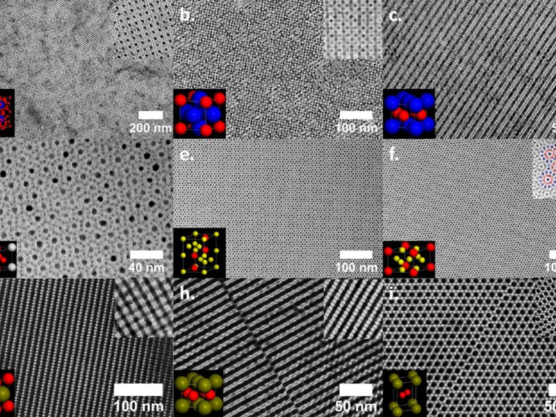
Polycatenar Ligands Control Nanocrystal Synthesis and Self-Assembly
Diroll, Jishkariani, Cargnello, C. Murray (Chemistry) MRSEC undergraduates Lizzy Dresselhaus and Natasha Iotov demonstrate diffraction of light to 6th-8th grade middle school girls participating in the Girls in Engineering Math and Science (GEMs) summer camp. (Kagan)
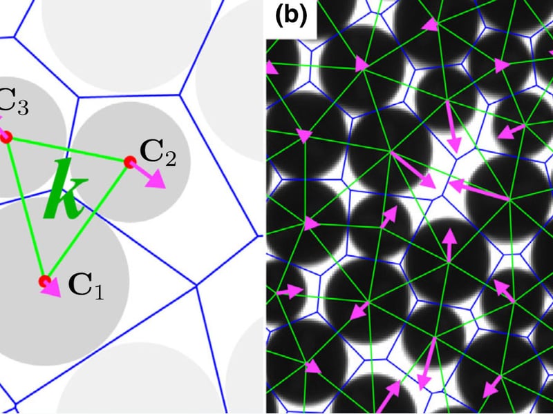
A new measure of structure in disordered materials
Douglas Durian and Andrea Liu (Physics)
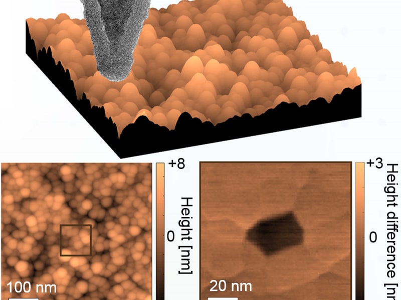
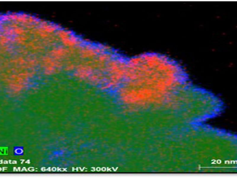
Heterogeneity in the small-scale deformation behavior of disordered nanoparticle packings
J. A. Lefever, T. D. B. Jacobs, Q. Tam, J. L. Hor, Y.-R. Huang, D. Lee (Chemical and Biomolecular Engineering), R. W. Carpick (Mechanical Engineering and Applied Mechanics)
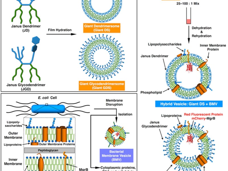
Hybrid Cell-Like Vesicular Assemblies from Bacterial Membranes and Synthetic Components
D. A. Hammer (Chemical Engineering), M. L. Klein (Temple, Chemistry), M. Goulian (Physics), V. Percec (Chemistry) Summer students, undergraduates, and high school students who contributed to the project
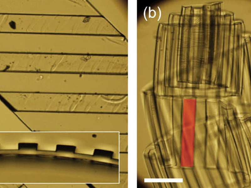
Three-dimensional Objects from Swollen, Topographically-Patterned Bilayer Films
R. D. Kamien (Physics), S. Yang (Materials Science & Engineering) and A. G. Yodh (Physics) Topography-guided buckling of swollen polymer bilayer films into three-dimensional helices. Based on physical constraints, simple surface topography can guide buckling of flat bilayer films to form objects such as half-pipes, helical tubules, and ribbons.
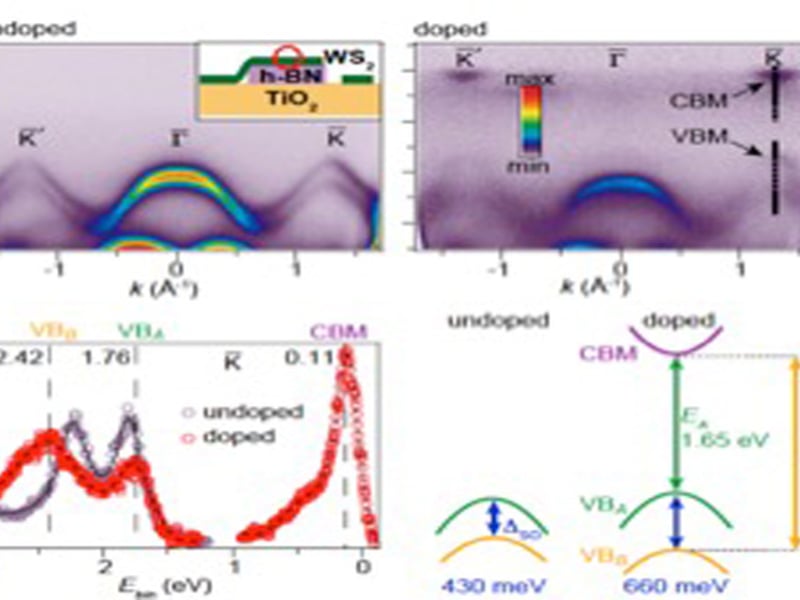
Control of Spin-Orbit Splitting in 2D Semiconductors
R. Kawakami, J. Goldberger, W. Windl The Ohio State University
Translating Spin Seebeck Effect Physics into Practice
S. R. Boona, K. Vandaele, I. N. Boona, D. W. McComb, and J. P. Heremans, "Observation of spin Seebeck contribution to the transverse thermopower in Ni-Pt and MnBi-Au bulk nanocomposites," Nature Communications 7, 13714 (2016). *supported by the Center for Emergent Materials, an NSF MRSEC (DMR1420451) and by MURI (W911NF-14-1-0016)
Through the Atomic Scale Looking Glass
Showing 561 to 570 of 1452