Highlights
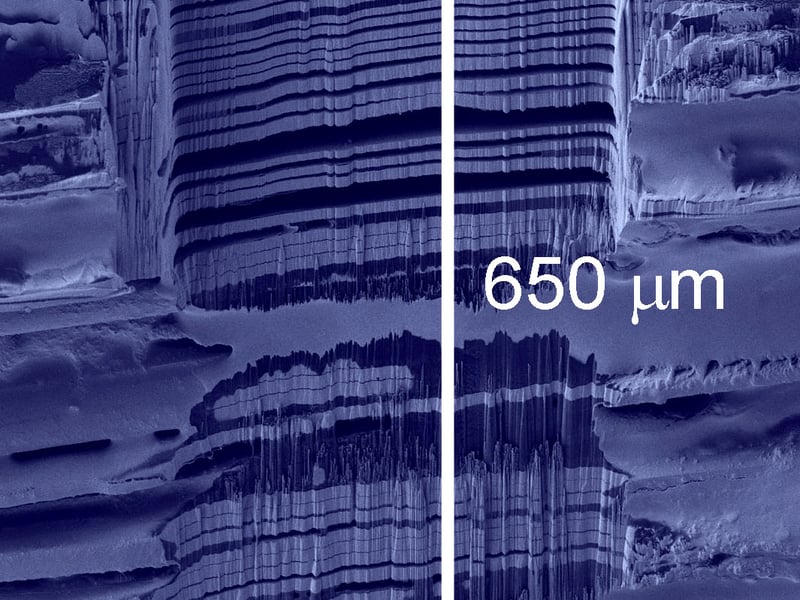
Focused Ion Beam / Scanning Electron Microscope: TESCAN S8000X
Eric A. Stach, Mark Allen, Marija Drndic and Deep Jariwala, University of Pennsylvania
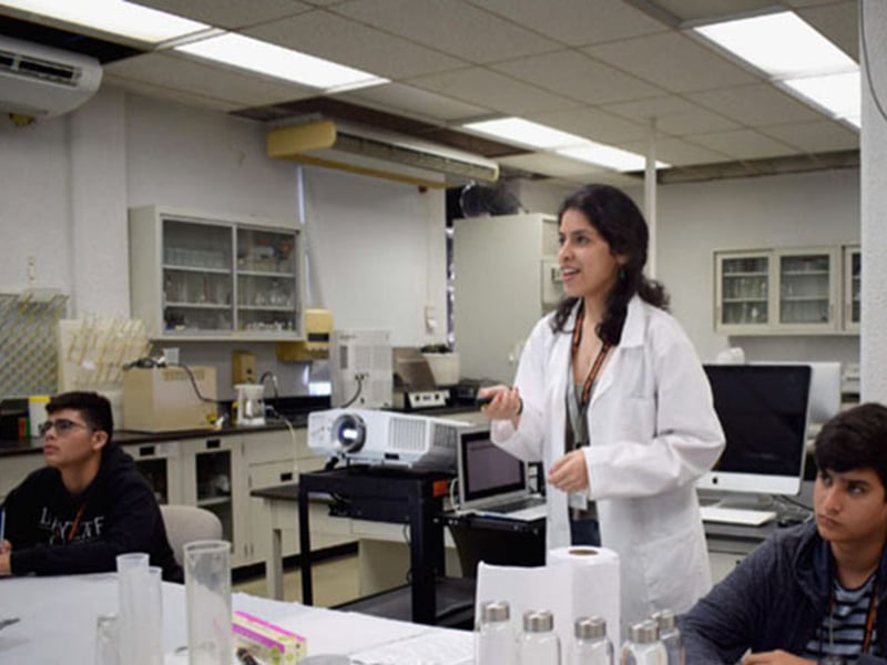
Experimenta con PREM
Mark Licurse & Ashley Wallace, University of Pennsylvania
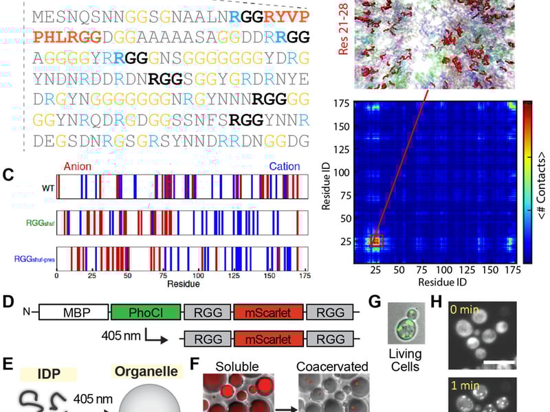
Membraneless Organelles Built from Engineered Assemblies of Intrinsically Disordered Proteins
Matthew C. Good, Daniel A. Hammer and Elizabeth Rhoades, University of Pennsylvania. Jeetain Mittal, Lehigh University
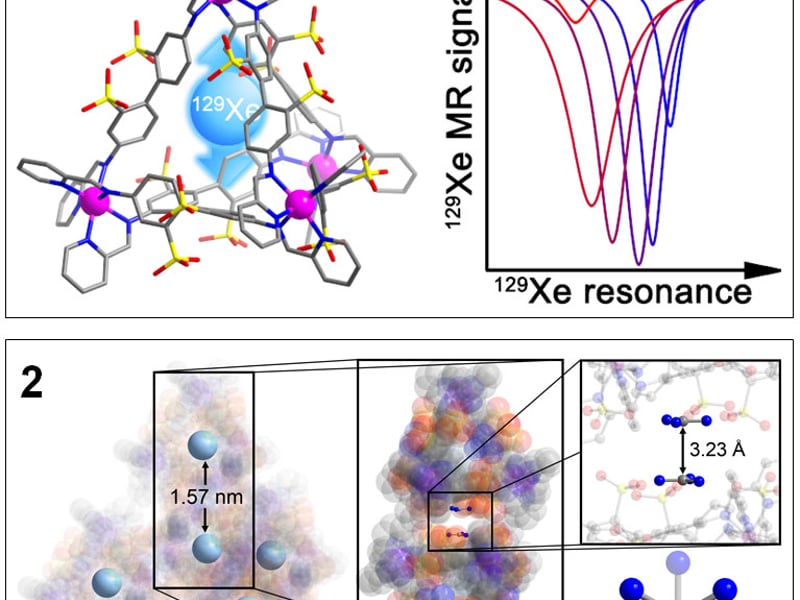
Paramagnetic Organocobalt Capsule Reveals Xe Host-Guest Chemistry
Kang Du, Serge D. Zemerov, Sebastian Hurtado Parra, James M. Kikkawa, Ivan J. Dmochowski, University of Pennsylvania
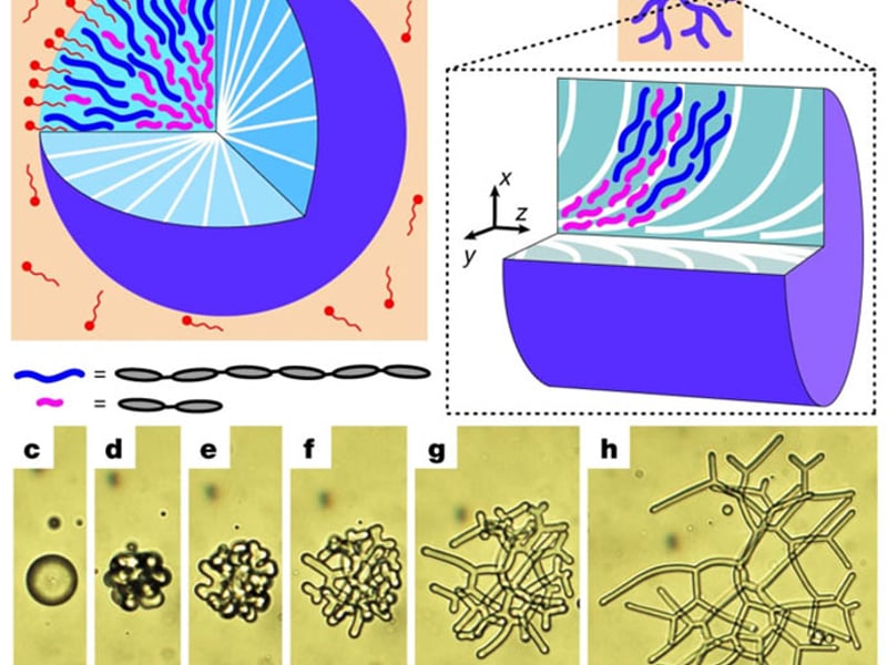
Molecular Heterogeneity Drives Reconfigurable Nematic Liquid Crystal Drops
W. S. Wei, Y. Xia, S. Ettinger, Shu Yang and A.G. Yodh, University of Pennsylvania
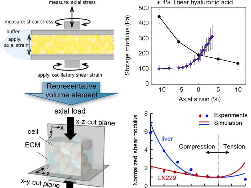
Emergence of Tissue-like Mechanics from Fibrous Networks Confined by Close-packed Cells
Anne van Oosten, Xingyu Chen, Vivek Shenoy, Paul Janmey, University of Pennsylvania
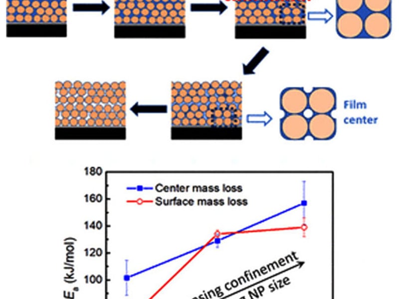
Thermal Degradation of Polymers under Extreme Nanoconfinement
H. Wang, Y. Qiang, A. A. Shamsabadi, P. Mazumder, K. T. Turner, D. Lee, Z. Fakhraai, University of Pennsylvania
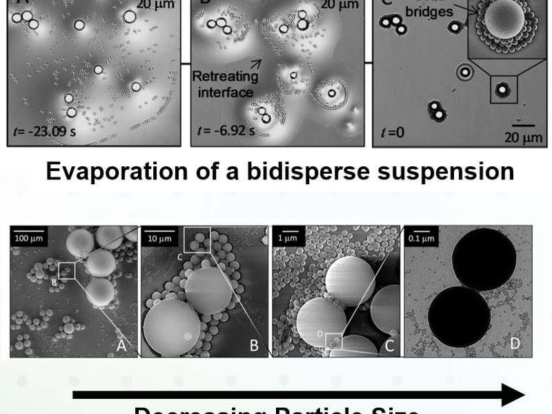
Formation of Stable and Hierarchical Particle Aggregates by “Solid Bridging”
A. Seiphoori, X-G Ma, P.E. Arratia, D. Jerolmack, University of Pennsylvania
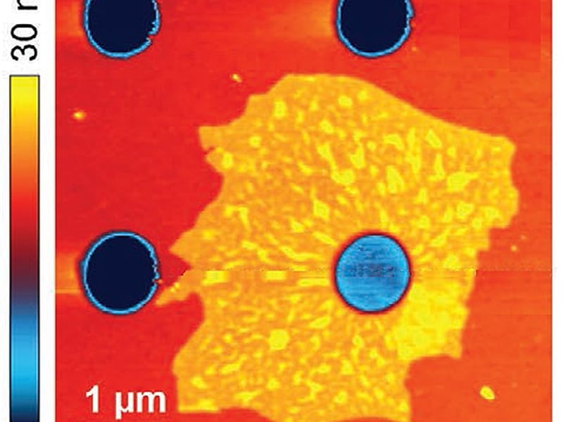
Nanoscale Properties of MXene Membranes
A. Sinitskii and A. Gruverman (University of Nebraska-Lincoln) and Y. Gogotsi (Drexel University)
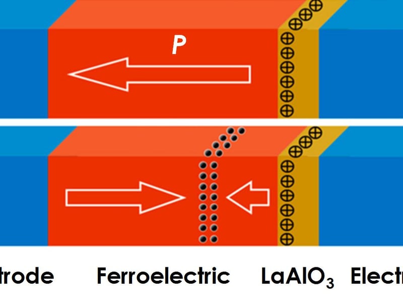
Ferroelectric Tunnel Junctions Enhanced by a Polar Oxide Barrier Layer
Qiong Yang, Lingling Tao, Evgeny Tsymbal, and Vitali Alexandrov (University of Nebraska-Lincoln)
Showing 321 to 330 of 1452