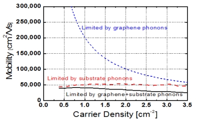
 Mobility measures how fast electrons travel in a material when an electric field (i.e. a voltage) is applied.Â’ At room temperature, the major limitation to mobility is vibrations of the lattice, called phonons, which scatter the electrons.Â’ UMD-MRSEC researchers measured for the first time the limits on mobility posed by the phonons in graphene (a single atom-thick layer of graphite), and found the graphene phonons extraordinarily weak, limiting the mobility to ~200,000 cm2/Vs at low charge carrier densities, more than 100 times higher than silicon, and higher than any known semiconductor.Â’ The effect of phonons in graphene is so weak that other effects, scattering by impurities and by phonons in the substrate below the graphene, are stronger.Â’ The work paves the way to higher mobility in graphene (by removing impurities, and using different substrates) which could lead to extremely high speed electronic devices.

Mobility Limits in Graphene
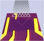
Top right: Optical image of graphene device (dark purple) contacted by gold electrodes (yellow) with a computer rendering of the graphene lattice above.
Bottom right: Mobility limits as a function of charge carrier density in graphene at room temperature, due to phonons in graphene (blue), optical phonons of SiO2 substrate (red), and the total due to both contributions (black).