Semiconductor nanocrystals are sensitive to air and solvents, which hinders wet-chemical processing under ambient conditions.
This problem has limited the scaling of nanocrystal device dimensions and large-scale device integration achievable by conventional processing.
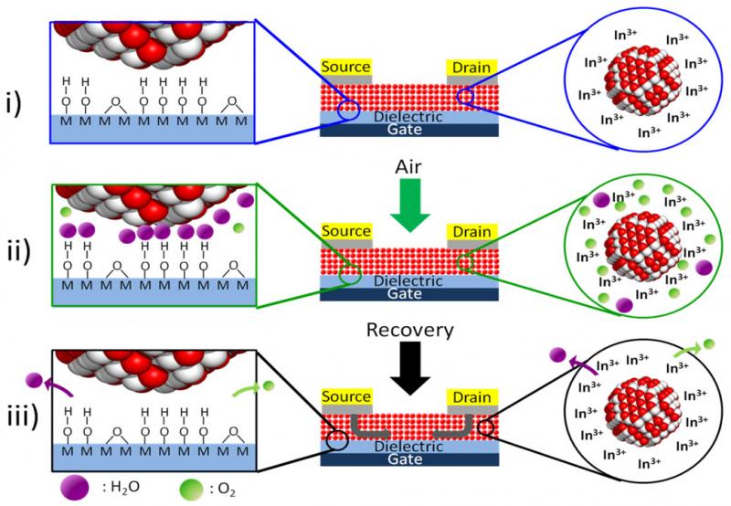
We demonstrated a simple, in-situ recovery route using indium metal as a chemical agent which upon thermal activation is triggered to diffuse and repair the damage introduced by chemical and environmental exposure that degrade the electronic properties of semiconductor NC thin films and their devices.

Figure 1 - Schematic of nanocrystal transistor recovery. (i) In-doped CdSe nanocrystals are (ii) exposed to air, adsorbing oxygen and water at the NC and gate oxide surfaces, and are (iii) recovered upon annealing under nitrogen, as oxygen and water desorb and additional indium diffuses in from the electrodes.