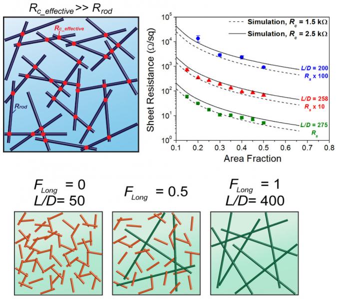
 Touchscreens are ubiquitous and transparent conductors make them possible. However, the cost and the physical limitations of indium tin oxide (ITO) are hampering progress toward flexible touchscreens. In this study (ACS Nano 2013) we demonstrate a new a way to design transparent conductors using metal nanowires that could enable less expensive — and flexible — devices.
A design challenge exists for nanowire transparent conductors, because more than thickness and bulk material’s properties are needed to predict properties. To determine the properties of nanowire networks, one needs to know the nanowires’ length and diameter, the area they cover and the contact resistance. How these four independent parameters impact the electrical and optical properties of nanowire networks has been unclear. We have combined experiments and modeling to extract the contact resistance between silver nanowires and used this value to explore the impact of nanowire length and areal density on sheet resistance and subsequently the optical transmittance.
Our modeling has quantified the interplay between the most critical parameters that govern performance in nanowire films, as well as set an important precedent in achieving quantitative correspondence between experiments and simulations in nanowire films so as to accelerate the advancement of these materials as transparent conductors.