Highlights
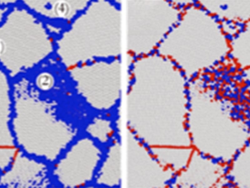
Machine Learning & Softness: Characterizing local structure and rearrangements in disordered solids
Paulo E. Arratia & Douglas J. Durian, University of Pennsylvania
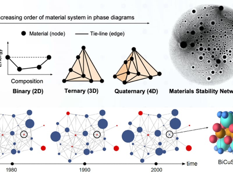
Network Analysis of Synthesizable Materials Discovery
Aykol et al. arXiv:1806.05772 (2018).
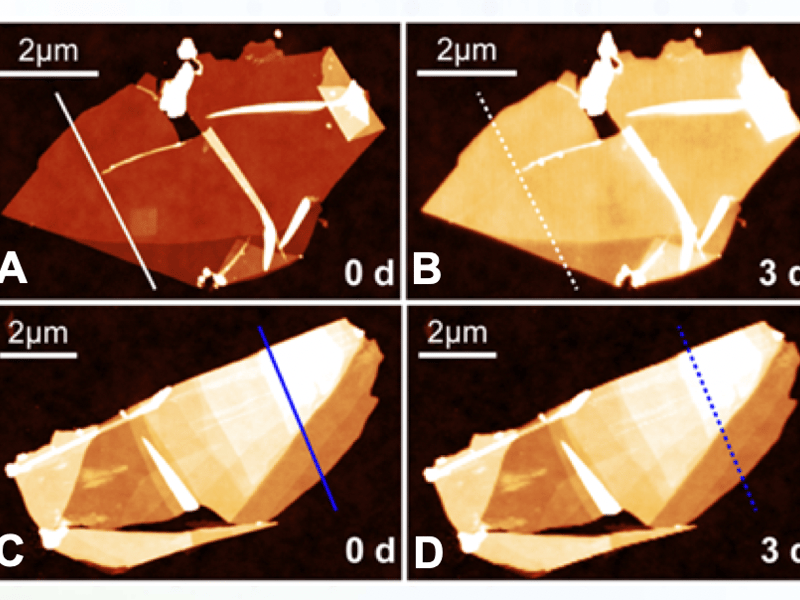
Improving the Ambient Stability of Chemically Reactive 2D Materials
S. A. Wells, A. Henning, J. T. Gish, V. K. Sangwan, L. J. Lauhon, and M. C. Hersam, “Suppressing ambient degradation of exfoliated InSe nanosheet devices via seeded atomic layer deposition encapsulation,” Nano Letters, 18, 7876-7882 (2018)
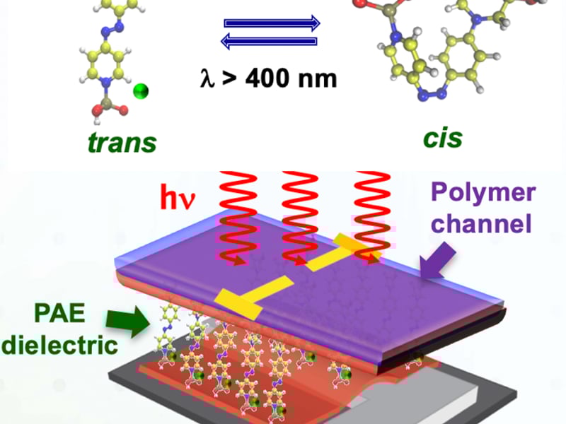
Optically Reconfigurable Dielectrics in Ultra-Thin Transistors
S. P. Senanayak, V. K. Sangwan, J. J. McMorrow, K. Everaerts, Z. Chen, A. Facchetti, M. C. Hersam, T. J. Marks, and K. S. Narayan, “Self-assembled photochromic molecular dipoles for high-performance polymer thin-film transistors,” ACS Appl. Mater. Interfaces, 10, 21492 (2018)
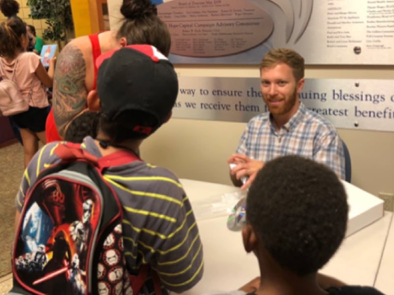
Reaching Underserved Audiences by Bringing Science to a Local Food Pantry
AnneLynn Gillian-Daniel, University of Wisconsin-Madison
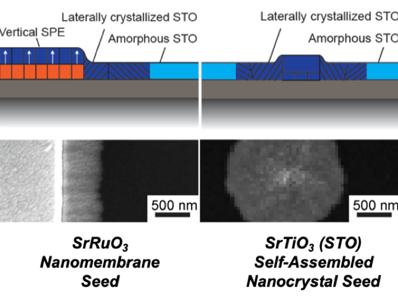
Nanoscale Control of Complex Oxide Crystallization
Paul Evans, Thomas Kuech, University of Wisconsin-Madison; Dillon Fong, Martin Holt, Argonne National Laboratory
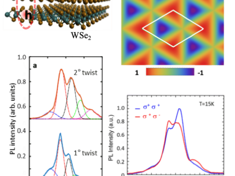
Optical Excited States in a Moiré Crystal
X. Li, A. H. MacDonald: University of Texas at Austin
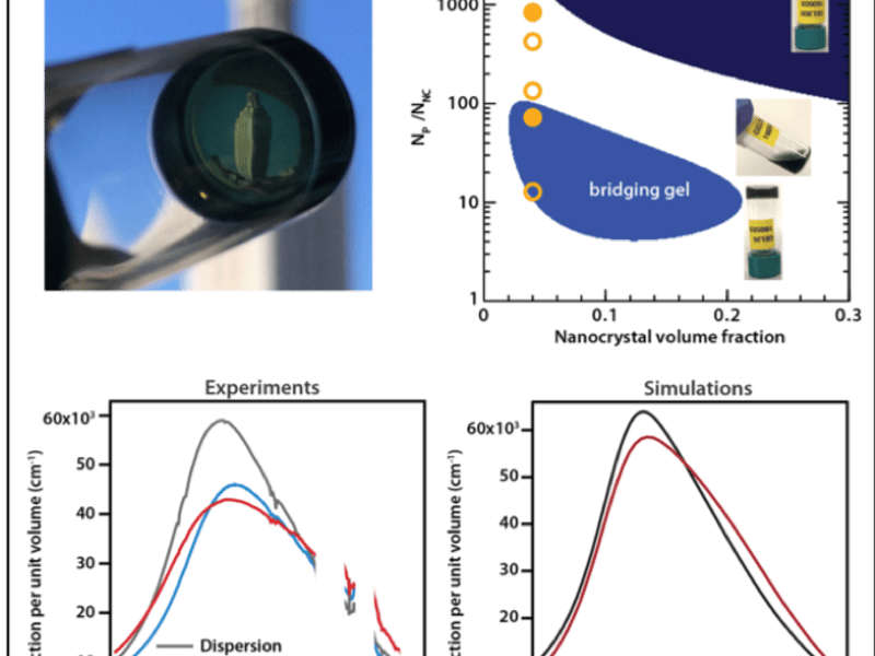
Gelation of Plasmonic Metal Oxide Nanocrystals by Polymer-Induced Depletion Attractions
Camila A. Saez Cabezas, Gary K. Ong, Ryan B. Jadrich, Beth A. Lindquist, Ankit Agrawal, Thomas M. Truskett, and Delia J. Milliron. GKO is affiliated to the department of Materials Science and Engineering at the University of California Berkeley. All other authors are affiliated to the McKetta Department of Chemical Engineering at the University of Texas at Austin.
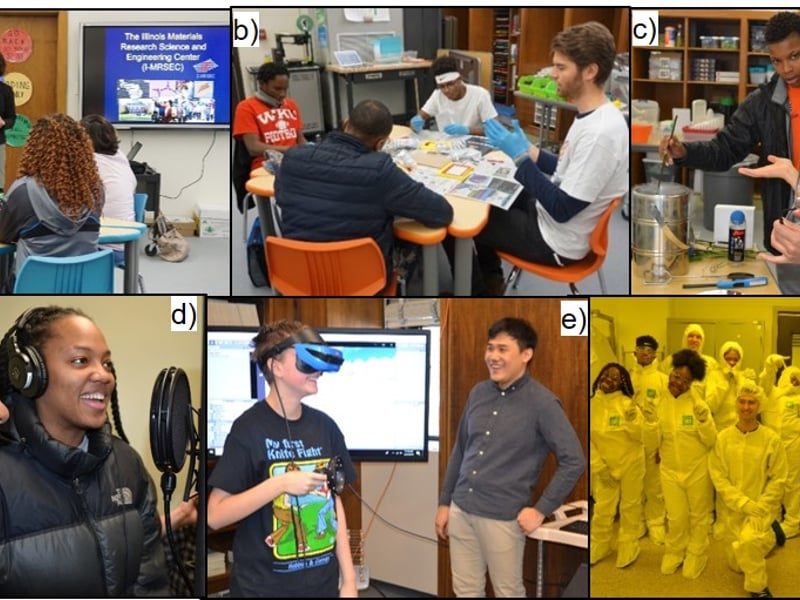
Musical Magnetism: Engaging Middle School Students in Materials Science
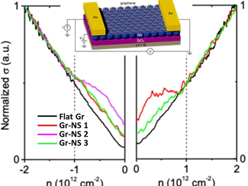
Strain Superlattice of Graphene on Nanospheres
N. Mason, N. Aluru, P. Huang, and M. Gilbert University of Illinois at Urbana-Champaign
Showing 401 to 410 of 1452