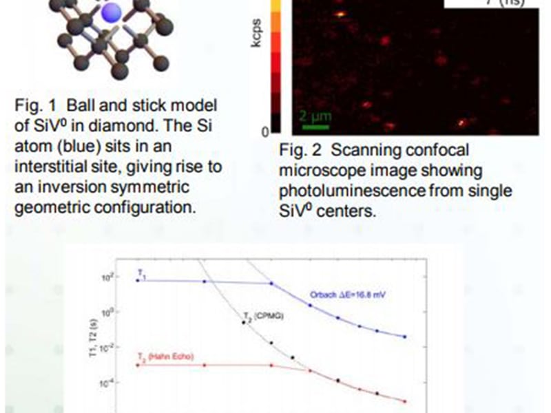
Highlights

Fig. 1  Optical micrograph of a superconducting photonic bandgap microresonator. This resonator geometry was a key advancement that enabled the study of electrically driven NMR
Fig. 2  Density plots showing coherent manipulation of 75As and 31P nuclear spins using only RF electric fields. Rabi oscillation” between the two spin states appear as the electric field control pulse amplitude or length is varied.
Fig. 1 Optical micrograph of a superconducting photonic bandgap microresonator. This resonator geometry was a key advancement that enabled the study of electrically driven NMR Fig. 2 Density plots showing coherent manipulation of 75As and 31P nuclear spins using only RF electric fields. Rabi oscillation” between the two spin states appear as the electric field control pulse amplitude or length is varied.
Aug 23, 2017
Princeton Center for Complex Materials (2014)

Electrical Manipulation of Nuclear Spins in Silicon

A. J. Sigillito, A. M. Tyryshkin, T. Schenkel, A. A. Houck, and S. A. Lyon, Princeton University

The spin degree of freedom for donor nuclei in silicon have exceptionally long coherence times making them useful as either quantum bits (qubits) or long-lived quantum memories. Nuclear spins are hard to control in nanoscale devices since they are thought to only be coherently manipulated using magnetic fields, which are hard to confine. In this collaboration, researchers in IRG3 identify two new physical mechanisms that allow for manipulation of nuclear spins using only electric fields.
Our findings will lead to a better understanding of the combined roles of interfaces, confinement and self-concentration effects on the properties of internally nanostructured polymers. The results will guide the development of next-generation copolymers with tunable interfacial properties.
Aug 22, 2017
Princeton Center for Complex Materials (2014)

Direct Measurement of the Local Glass Transition in Nanophase Structured Copolymers with One Nanometer Resolution

R.A. Register (Princeton) and R. D. Priestley (Princeton)

Block copolymers, which self-assemble into nanostructures due to the incompatibility of each block, have generated intense scientific interest and are used in a myriad of important technologies.  In such systems, the majority of the macromolecules can lie within a few nanometers of an internal interface, within a region where the dynamics and mechanical properties can be highly modified from their bulk values.
We expect that this study will provide insight into the design of next-generation industrial polymer processing, where nanoscale control of the structural heterogeneities of semi-crystalline phase is crucial.
Aug 22, 2017
Princeton Center for Complex Materials (2014)

Dramatic Tunability in Melting Temperature and Crystallinity of Polyethylene by Exploiting Confinement During Processing

R. D. Priestley (Princeton), C. B. Arnold(Princeton), Y.-L. Loo(Princeton) and R. A. Register (Princeton).

We exploited Matrix Assited Pulsed Laser Evaporation (MAPLE) to deposit polyethylene from a quasi-vapor phase at a controlled substrate temperature, to crystallize polymers under confinement at a wide range of target crystallization temperature, Tc.  The team showed the remarkable controllability of the semi-crystalline structure of PE by MAPLE with the control of substrate temp.; see Figure A and B. In comparison to melt-crystallized PE (Fig.
Local density of states on the surface of bismuth at magnetic field B = 12.9 T and energy E = 780 µeV. Dark concentric ellipses reflect the shape of individual electronic states. The anisotropy points in different directions for states at other energies.
Aug 21, 2017
Princeton Center for Complex Materials (2014)

Real-space imaging of a nematic quantum liquid

B. E. Feldman1, M. T. Randeria1, A. Gyenis1, F. Wu2, H. Ji1, R. J. Cava1, A. H. MacDonald2, A. Yazdani1 1Princeton University 2University of Texas at Austin

Interactions among electrons can give rise to a variety of exotic quantum phases in solids. An intriguing example is the formation of “nematic” electronic states, whose wave functions break the rotational symmetry of the host material. By examining electronic behavior on the surface of bismuth at high magnetic field, the Princeton MRSEC group showed that a combination of strain and electron-electron interactions lifts the degeneracy of electronic states in this material.
Figure 1: Curves showing how the resistance at selected temperatures falls with increasing magnetic field B in GdPtBi. The decrease reflects the emergence of the axial current, an effect called the chiral anomaly (Ref. 2). The curves in Na3Bi (1) are remarkably similar.
Aug 21, 2017
Princeton Center for Complex Materials (2014)

Chiral anomaly observed as an axial current in two topological quantum materials

M. Hirschberger (Princeton), J. Xiong (Princeton), S. Kushwaha (Princeton), A. Bernevig (Princeton), R. J. Cava (Princeton), and N. P. Ong (Princeton)
Electrons in topological materials behave like massless particles (called Weyl fermions). They are either right- or left-handed (the spins are locked parallel or antiparallel to their velocity). In parallel applied electric and magnetic fields, one population grows while the other shrinks. This leads to a new kind of electrical current called an “axial” current. The Princeton MRSEC group has observed this new effect (called the chiral anomaly) in two distinct topological metals, Na3Bi and GdPtBi (1,2).
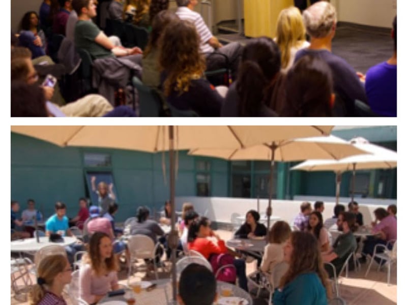
(Top) Winter 2017‒Dow Distinguished Lecturer Temple Grandin speaking to a packed room.
(Bottom): UCSB graduate & California State University  students mingling during lunch
(Top) Winter 2017‒Dow Distinguished Lecturer Temple Grandin speaking to a packed room. (Bottom): UCSB graduate & California State University students mingling during lunch
Jul 19, 2017
Materials Research Science and Engineering Center at UCSB

Graduate Students for Diversity in Science at UCSB

Ram Seshadri, UCSB  
Graduate Students for Diversity in Science is composed of an interdisciplinary group of young scientists at the University of California, Santa Barbara (UCSB). The cornerstone of the group lies in its recognition of the cultural heritage and diversity of many exceptional scientists who have set foundations through research, service, and leadership in their respective disciplines and across many boundaries. GSDS aims to promote participation in the science, technology, engineering and math (STEM) fields and foster an inclusive atmosphere that celebrates diversity.
Jul 19, 2017
Materials Research Science and Engineering Center at UCSB

DNP Nuclear Magnetic Resonance

Ram Seshadri, UCSB  
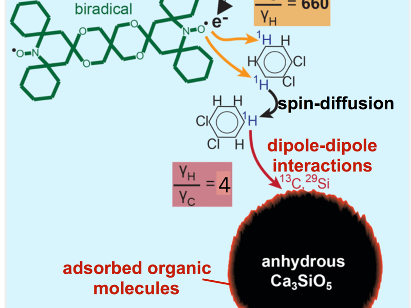
The DNP-NMR technique in the MRSEC Shared Experimental Facilities allows the selective measurement of surface species, in addition to enabling large sensitivity enhancements. The biradicals serve only to act as an antenna for the microwaves. Very small quantities of biradicals are introduced into the sample, which do not change the surface chemistry that results from hydration.
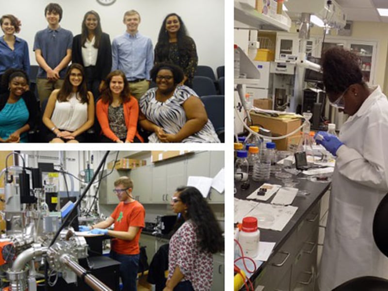
(Top Left): 2016 C-PHOM High School Research Program Participants. (Bottom Left): 2016 High School student working in the lab with Grad mentor. (Right): 2016 High School student working in the lab.
Jul 12, 2017
Center for Photonic and Multiscale Nanomaterials (2011)

From High School to Professional Scientist: Developing a Pipeline

Akesha C. Moore* and Rachel S. Goldman** *EECS Department, **MSE Department, University of Michigan

With declining numbers of STEM degrees and limited diversity in the STEM workforce, there is a need for expansion of research opportunities for undergraduate and high school students, in particular those from underrepresented groups.
(a) SEM image of a nanowire array. (b) SEM image of the fabricated photonic integrated circuit. (c) TEM images of single nanowires showing the formation of quantum dot-like nanostructures in the InN disk regions.
Jul 12, 2017
Center for Photonic and Multiscale Nanomaterials (2011)

1.3µm Optical Interconnect on Silicon: A Monolithic III-Nitride Nanowire Array Photonic Integrated Circuit

Prof. Pallab Bhattacharya, University of Michigan, Ann Arbor

A feasible optical  interconnect on a silicon complementary metal-oxide-semiconductor chip demands epitaxial growth and monolithic integration of diode lasers and optical detectors with guided wave components on a (001) Si wafer, with all the components preferably operating in the wavelength range of 1.3–1.55 μm at room temperature.
Jul 12, 2017
Center for Photonic and Multiscale Nanomaterials (2011)

Generating Accelerating Light with Metasurfaces

University of Michigan (U-M) and Purdue University (P-U)

Finely patterned surfaces, known as metasurfaces, can control light with unprecedented ability. Unlike traditional optical elements, metasurfaces derive their optical properties from their subwavelength texture rather than their shape.