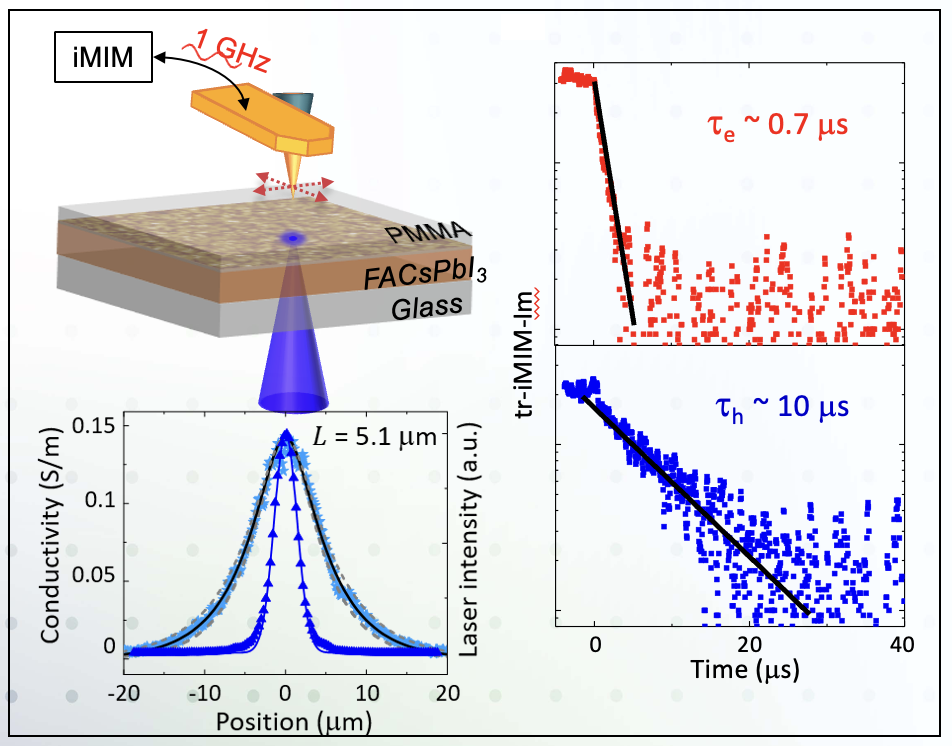
 This highlight illustrates a key characterization advance realized at the Center for Dynamics and Control of Materials – temporally resolved light-induced microwave impedance microscopy (MIM). In MIM, microwave-frequency dielectric response is measured with nanoscale spatial resolution by an atomic force microscope probe tip functionalized with a microwave strip line. In temporally resolved light-assisted MIM, modulated or pulsed laser illumination of the tip-sample junction enables dielectric response associated with photogenerated carriers, e.g., photoconductivity, to be measured with high spatial and temporal resolution. In the experiments shown here, this technique is used to probe the diffusion lengths and recombination lifetimes of electrons and holes in organic-inorganic hybrid perovskite materials, specifically Cs-doped FAPbI3, of intense current interest for photovoltaic applications. Device structures containing either electron or hole transport layers enable the dynamics of electrons and holes to be separated. These measurements provide key insights into material properties that strongly influence the performance of organic-inorganic hybrid perovskite materials in photovoltaic devices.