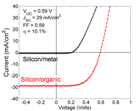
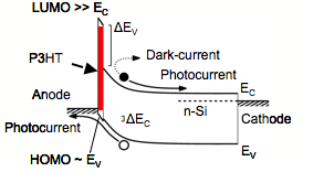
 In a photovoltaic cell, an incident photon creates an electron (black circle in top sketch) and a hole (open circle). For maximum efficiency, the opposite charges should be swept to opposite electrodes of the device (arrows) before they have a chance to recombine. The efficiency is further enhanced if a wide band gap organic semiconductor (e.g. P3HT) is grown on the surface of silicon. The wide gap (shown in red) blocks electrons from spilling into the anode. Organic semiconductors provide great design flexibility in tuning band offsets. A challenge, however, is controlling the defects (dangling bonds) at the interface with Si, which degrade device performance. PCCM scientists Sturm, Kahn, Loo and Schwartz have solved the surface passivation problem, and have achieved quite high efficiencies (~10%) in hybrid devices. An important advantage is that these devices can be made at low temperatures (o C).