We
have achieved a successful molecular beam epitaxy growth of Bi2Se3 / ZnxCd1-xSe
superlattices in which topological properties of individual 10 nm thick TI
layers are enhanced. ZnxCd1-xSe (ZnCdSe) is a `trivial’
wide band gap II-VI group semiconductor with a 2.12 eV band gap and a nearly
perfect lattice match to Bi2Se3. We demonstrated that in these
superlattices a two-dimensional (2D) weak antilocalization quantum correction
to classical magneto-resistance associated with topological Berry phase scales
with the number of TI layers, having one quantum channel per layer obtained
from the fits to 2D localization theory. The choice of layers abutting
topological surfaces can be critical. The robustness of our multilayer
topological structure and the ZnCdSe (wurtzite) crystal structure that induces
interfacial electronic asymmetry show that surface charge transfer and the
corresponding bending of 2D-like subsurface bulk bands can be controlled.
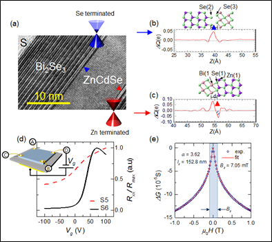
(a) HRTEM image of a superlattice (grown on a sapphire
substrate, S). Zn-terminated (red arrow) and Se-terminated (blue arrow) interfaces
are marked on the image. DFT calculated charge transfer at (b)
Se-terminated interface of ZnCdSe with a TI Bi2Se3 (blue arrow) and at (c) Zn terminated
interface (red arrow). Our experiments
and band structure calculations demonstrate that Se-termination does not induce
interfacial charge transfer and hence a formation of the 2DEG states, but
Zn-termination does (hatched region of negative DQ in (c). (d) The effect of Zn dangling bonds
and charge transfer is clearly seen in the shift of Dirac point corresponding
to the maximum of longitudinal resistance Rxx vs. gate voltage Vg. Here
the red curve (sample S5) is with interfacial Zn and black curve (sample S6) is
without. This demonstrates that the interfacial asymmetry induced by a suitable
crystal structure of the spacer layer (here ZnCdSe is wurtzite) can guarantee
that only one interface remains topological. (e) This is confirmed by
the quantum interference correction to the 2D conductance measurements which
scales with the number of TI layers in the superlattices and has only one
quantum conductance channel per layer.