It was recently discovered that Graphene – a two-dimensional sheet of carbon atoms – possesses a room temperature electron mobility higher than any other known material. This discovery was honored by the 2010 Nobel Prize in physics. Graphene is now imminent as the suitable candidate for high speed nanoscale field-effect transistor devices. With contemporary semiconductor technology stretched to its scaling limits, graphene could be immediately employed for realization of a new generation of electronic devices, deposited by onto large-area substrates. The major problem to overcome is the lack of understanding and control of the influence of the substrate onto the electrical properties of epitaxial graphene. Researchers at the University of Nebraska MRSEC in collaboration with their colleagues from the Naval Research Laboratory have reported optical determination of free-charge carrier mobility, sheet density, and resistivity parameters in epitaxial graphene at room temperature. [Applied Physics Letters 98, 041906 (2011)] Using high-frequency optical-Hall effect measurements they found that surface orientation strongly influences the carrier channel formation. This finding may open pathways to achieve extreme carrier density and mobility at high frequencies in epitaxial graphene, and thus could trigger a revolution in high-speed electronic devices.

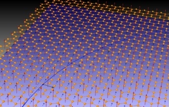
The path of a free charge carrier across a sheet of graphene deposited on a silicon carbide substrate, subjected to a magnetic field. The free charge carriers are accelerated within the electric field of a high-frequency wave thus diverting from a transverse path which produces the Optical Hall effect.