In nanoscale devices, we have the opportunity to isolate the individual physical processes of noise.Â’ Â’ Time-resolved STM imaging of fluctuating nanoscale structure shows that the motion of surface line boundaries (steps) is coupled 10x more strongly to scattering of electrical carriers than predicted from zero-temperature calculations.Â’ The resulting changes in surface resistivity will carry the spectral characteristic of the step fluctuations, yielding a distinct noise signature SI ~ f-3/4.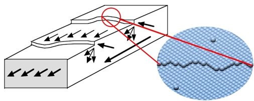
Scattering at Nanoscale Structure in Metals
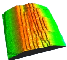
Top above: Scanning Tunneling Microscope (STM) image of the top of a 20 nm diameter crystalline Ag wire. The longitudinal structures are steps - changes in height by a single atomic layer.
Middle above: Schematic illustration of the scattering of charge carriers at surface steps, with expanded image illustrating the thermal excitations of the atomic structure that cause step motion.
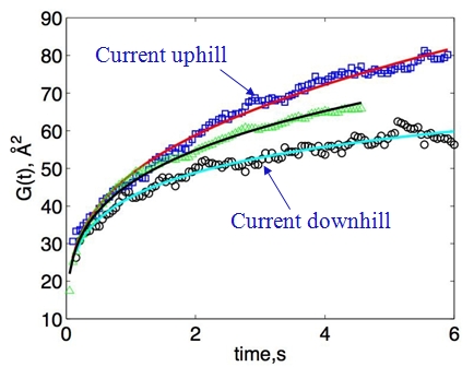
Bottom left: The thermal motion of the steps, shown by the correlation function G(t), is enhanced or suppressed when current flows uphill or downhill with respect to the step direction.