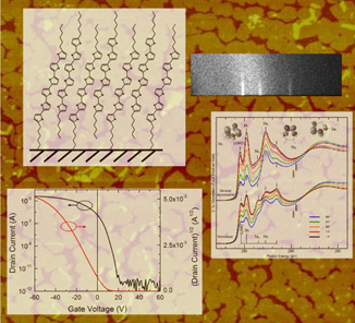
 The electronic properties of thin films with thicknesses of only a single molecular layer have in the past typically been far worse than thicker films of the same material. Recent studies by IRG2 of the Wisconsin MRSEC have now discovered that monolayer-thickness two-dimensional layers of α,ω-dihexylsexithiophene (α,ω-DH6T) exhibit field-effect hole mobility of up to 0.032 cm2 V-1 s-1, higher than previously reported for monolayers of other small-molecule organic semiconductors. In situ measurements during deposition show that the source-drain current saturates rapidly after the percolation of monolayer-high islands, indicating that the electrical properties of α,ω-DH6T transistors are largely determined by the first molecular monolayer. The α,ω-DH6T monolayer consists of crystalline islands in which the long axes of molecules are oriented approximately perpendicular to the plane of the substrate surface (see Figure below). In-plane lattice constants measured using synchrotron grazing-incidence diffraction are larger in monolayer-thickness films than the in-plane lattice constants of several- monolayer films and of previously reported thick-film structures. Near-edge X-ray absorption fine structure spectroscopy (NEXAFS) reveals that the larger in-plane tlattice constant of single-monolayer films arises from a larger tilt of the molecular axis away from the surface normal. NEXAFS spectra at the C 1s and S 2p edges are consistent with a high degree of molecular alignment and with the local symmetry imposed by the thiophene ring. The high mobility of holes in α,ω-DH6T monolayers can be attributed to the reduction of hole scattering associated with the isolation of the hiophene core from the interface by terminal hexyl chains. The NEXAFS results were obtained by people from IRG3 of the Wisconsin MRSEC.