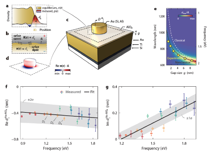
 Local, bulk response functions, e.g. permittivity, and the macroscopic Maxwell equations completely specify the classical electromagnetic problem, which features only wavelength and geometric scales. They have proven extremely successful at macroscopic length scales, across all branches of photonics. Even state-of-the-art plasmonic studies, exemplars of extremely interface-localized fields, rely on their validity.
This classical description, however, neglects the intrinsic electronic scale associated with interfaces. This omission leads to significant discrepancies between classical predictions and experimental observations in systems with deeply nanoscale feature sizes, typically evident below ∼10 – 20 nm.
The d parameters are a convenient parametrization for surface-related, quantum corrections. We establish a systematic approach to measure the d parameter dispersion of a general two-material interface. This approach enables the first measurement of the dispersion of the d parameters of an interface.