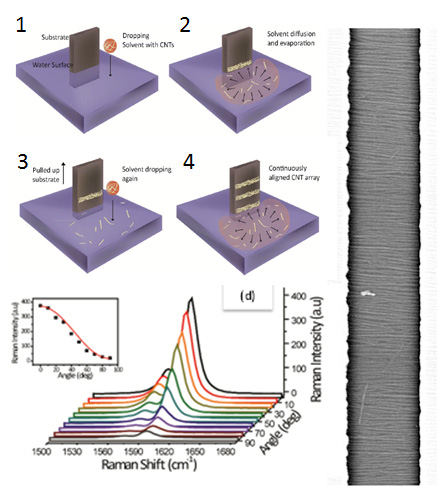
 Creating aligned arrays of high purity (>99.9%) semiconducting single-walled carbon nanotubes (s-SWCNTs) over a large area has been a significant challenge in materials synthesis. Towards this goal, IRG2 have recently developed a novel yet simple method to deposit aligned s-SWCNTs on substrates via dose-controlled, floating evaporative self-assembly. The diffusion of organic solvent at the water-air interface results in the deposition aligned s-SWCNTs on a partially submerged hydrophobic substrate, which is withdrawn vertically from the surface of water, hence gaining complete control over where the stripes are deposited and the quantity of s-SWCNTs deposited. Polarized Raman studies have shown that the s-SWCNTs are aligned within ±14º, are packed at a density of 50 s-SWCNTs µm-1.
The result is the rapid deposition of s-SWCNTs into aligned arrays that can be adapted for scalable integration into a wide variety of microelectronic applications. Already field-effect transistor (FET) devices show high performance with a mobility of 38 cm2 V-1 s-1 and on-off ratio of 2.2 × 10⁶ at a channel length of 9 μm.