The term “defect” suggests something to be avoided. However, our team has developed an extensive toolkit to control the locations, shapes, and detailed geometry of so-called topological defects in liquid crystals, the same sorts of materials used in the $100bn/year display industry. Our goal is to harness these defects to use them as cues for further directed- and self-assembly, as lenses and optical elements, and as building blocks for hierarchical materials.

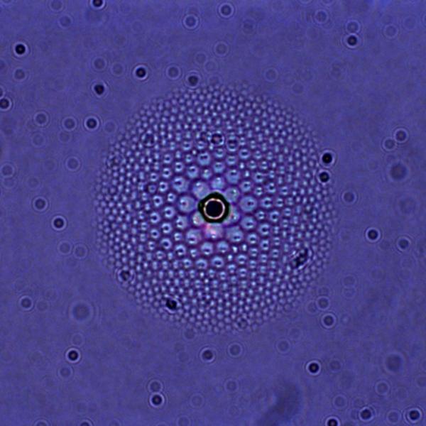
We plant a silica bead (center) in thin smectic film. The surface tension on the bead leads to a curved air/smectic interface. To satisfy the equal spacing condition of the smectic layers, focal conic domains are formed of varying eccentricity and size. These petals are arranged in a tiered, convex fashion and, because the liquid crystal can interact with light, the entire assembly can function as a lens, focusing light.
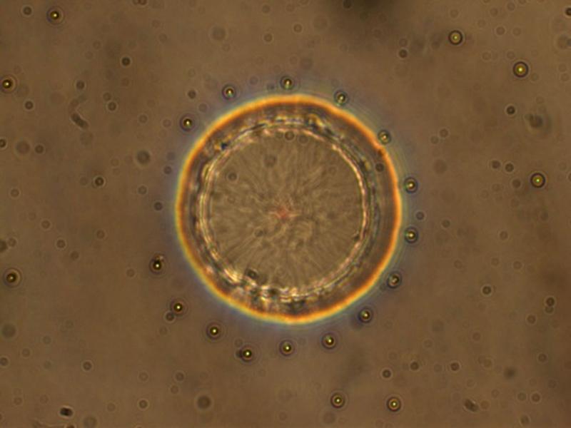
 We start with a template consisting of microscopic posts that was then topped with nematic liquid crystal. In this experiment a ring-shaped defect encircled each of the posts at their midpoints. This ring then acts like another template, directing the arrangement of patterns on the liquid crystal surface, more than 50 microns away.