The wide range of instrumentation within the University of Wisconsin MRSEC Shared Instrumentation Facilities (UW-MRSEC SIF) can now be accessed by academic and industry users around the nation via the Materials Research Facilities Network (MFRN.org). A Significant new addition over the past year is a Cameca LEAP 3000 Si ATOM Probe.
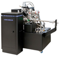 The Cameca LEAP 3000 SI atom probe microscope was installed in February 2014. The Atom probe microscope (shown at the left) provides nano-scale surface, bulk and interfacial materials analysis of simple and complex structures with atom-by-atom identification and accurate spatial positioning, also known as Atom Probe Tomography (APT). The LEAP is expected to be used heavily by MRSEC researchers in all IRGs to investigate the structure of interfaces at the nanoscale.
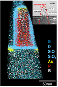 An example of the power of the LEAP, Inoue et al.1 have investigated 3D dopant distributions in an n-MOSFET. Regions of the device analyzed include the gate, gate oxide, channel, source/drain extension, and halo. The atom map to the right shows the data set along with a TEM image of the analyzed region of the transistor (inset). Arsenic atoms (in yellow) are visible in the source/drain extension and on top of the gate electrode. The As concentration in the source/drain extension was 2×1021 cm-3 with As atoms being detected to a depth of ~10 nm from the implanted Si surface. B atoms (in white) can be seen in the Si substrate (channel and halo extension regions), the boron concentration in the channel region was measured to be 1×1018 cm-3.