 Atom probe tomography for 3D discovery
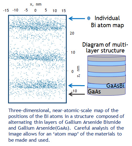
General Overview: Electronic devices inside of our cell phones and laptops are comprised of many precisely controlled layers formed by a process called “chemical vapor deposition”. Atoms from a gas react and deposit on a surface where they organize into a crystal. By utilizing two atom-level microscopes, a high-resolution scanning transmission electron microscope and a new three-dimensional atom mapping probe, a group of researchers at University of Wisconsin-Madison, have demonstrated that it is possible to ‘see’ whether the atoms are uniformly distributed or form atom-level clusters. In particular, they have “looked” at a new semiconductor, Gallium Arsenide Bismide, that is made out of elements that do not want to mix. Even though the Bismide in this material does not want to be part of the crystal, the researchers have used their atom-scale imaging capabilities to discover conditions whereby this ‘oil and water’-like mixture can form a homogeneous material. This is providing access to an entirely new range of semiconductor materials.