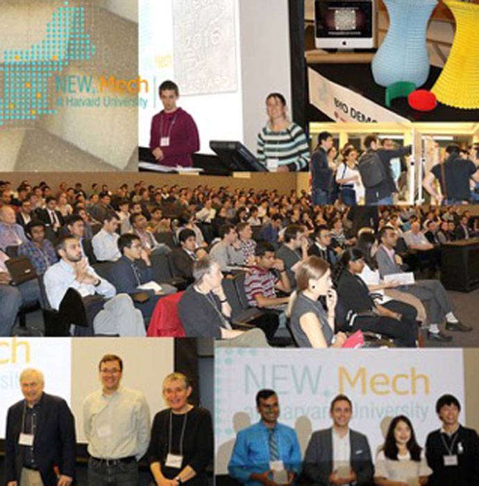
Skip to content Skip to navigation

Program Highlights for year 2020

Interfacing with Topological Crystalline Insulators

We demonstrate a route to high quality interfaces between IV-VI PbSnSe and conventional III-V semiconductors, offering means to host and manipulate electronic states that arise at this interface. We can now clarify the extent to which topological protection from backscattering persist in systems at relevant length scales for logic and interconnects using these novel materials.

Point Defects in hexagonal BN for Quantum Information Science

Hexagonal boron nitride is a suitable host for single-photon emitters and single-spin centers.  Strong single-photon emission has been observed, but the source was not identified.  Based on advanced first-principles simulations, the origins have now been pinpointed: the 2 eV emission has been attributed to boron dangling bonds, and 4 eV emission to carbon-carbon dimers.

Microstructure modeling in nonsolvent induced phase separation (NIPS) 

NIPS is a non-equilibrium liquid-liquid phase separation phenomenon used to make polymer membranes through solvent-nonsolvent exchange. Newly developed phase-field simulations allow investigation of coupled mass transfer, flow and thermodynamic instability during processing and the corresponding microstructures that result from variations in film composition and thickness.

Controlling skyrmion size in the alloy FePd1−xPtxMo3N

After discovering a new magnetic host of skyrmion states, UC Santa Barbara IRG-1 researchers were able to show that chemically alloying the compound FePd1−xPtxMo3N allows for the size of the skyrmion defects to be controlled while still preserving their stability.

Computational Design of Triblock Amphiphiles with 1-nm Domains

Block polymers are a class of versatile self-assembling soft materials that can form exquisite nanostructures for applications including ion transport membranes for batteries and fuel cells, and templates for inorganic oxide catalysts.

From Semiconductor to Metal in Two-dimensional Tellurium

Atomically-thin sheets of semiconductors have been of immense interest since the Nobel-Prize-winning discovery of graphene or two-dimensional (2D) carbon. Such materials represent the ultimate limit of “scaling” to small sizes, of vital importance in the semiconductor device industry.

Breakthrough in materials for actuators paves way to electronically integrated microscopic robots

Fifty years of Moore’s Law scaling in microelectronics have brought remarkable opportunities for the rapidly-evolving field of microscopic robotics. Electronic, magnetic, and optical systems now offer an unprecedented combination of complexity, small size, and low cost, and could readily be appropriated to form the intelligent core of microscopic robots.

High-conductivity 2D holes induced by polarization discontinuity in GaN/AlN

When an electrically-insulating material is grown on top of another insulator, the interface between the two insulators can be populated by mobile electrons. This has been achieved in interfaces that have a polarization discontinuity, such as AlGaN/GaN and LaAlO3/SrTiO3.

Designing the flow properties of concentrated particle suspensions

In a concentrated suspension of small solid particles in a liquid under shear, a large number of dynamically evolving particle-particle and particle-liquid interfaces controls the overall flow properties.

Wafer-scale synthesis of monolayer two-dimensional porphyrin polymers

At the University of Chicago MRSEC, Park and Sibener developed a synthesis of two-dimensional (2D) polymers with wafer-scale homogeneity, one monolayer thick, using a general and scalable growth method called laminar assembly polymerization.

Pages