Highlights
Mar 9, 2009
Massachusetts Institute of Technology
Fundamental MIT MRSEC research enables life-saving technology
Yoel Fink (MIT), John Joannopoulos (MIT), Edwin Thomas (MIT)
Technology based on fundamental studies carried out within our MRSEC is
now saving lives at hospitals across the country: over 175 novel
endoscopic surgical procedures per week are being carried out across
250 medical facilities in the U. S. using high-power laser radiation
delivered by OmniGuide photonic fibers.
Feb 13, 2009
Carnegie Mellon University
PREM Collaboration yields scientific and educational results
Robert Smith, Rufina Alamo, and Michael Bockstaller
A collaboration between PREM partners, Michael Bockstaller (CMU) and Rufina Alamo (FAMU) had great outcomes for both science and education. A student from Alamos's group at FAMU, Robert Smith, joined Bockstaller's group during the summer to study the effect of selective chlorine substitution on the crystallization of polyethylene. Scientifically, the collaboration resulted in two publications co-authored by Smith, Bockstaller, Alamo, and others (see figures below). Educationally, Smith's exposure to graduate research at CMU led him to apply for graduate school at CMU and elsewhere.
Feb 13, 2009
Carnegie Mellon University
Grain Boundary Lifetimes
Shen Dillon and Gregory Rohrer
The types of grain boundaries that make up the interfacial network within polycrystalline solids influence the properties and performance of the material. The population of grain boundary types is anisotropic, meaning that some of the types are found more frequently than others.
Jan 28, 2009
Princeton University
Adhesion and Interfacial Fracture in Soft and Hard Materials
Kurt Wolf, Arjenta Orana, Roy Fennimore, George Papandreou, and Cynthia Maryanoff (Johnson & Johnson)
One of the challenges in developing robust multilayers is the need to predict the interfacial strength between hard and soft materials. For example, in the case of drug eluting stents that are being used increasingly to treat arteriosclerosis, there are concerns that the drug-eluting layer may detach from the polymeric layers that are used to attach the soft drug eluting layers to the hard metallic stent substrate.
Jan 28, 2009
Ohio State University
Toward Site-Specific Stamping of Graphene
D. Li, W. Windl and N.P. Padture, The Ohio State University
A physical hypothesis based on theory and ab initio modeling for the stamping of graphene and few layers graphene (FLG) on silica is presented, and the feasibility of site-specific stamping of FLG patterns is demonstrated experimentally (figure below shows 10-layer FLG pattern stamped on silica). The site-specific nature of the patterned stamps over large areas could enable high-throughput fabrication of future graphene-based integrated devices.
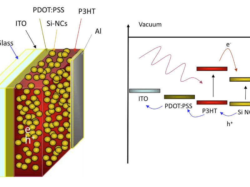
Jan 21, 2009
University of Minnesota - Twin Cities
Hybrid Silicon Nanocrystal-Polymer Solar Cells
Uwe Kortshagen
Mr. Chin-Yi Liu, a graduate student working in Professor Kortshagen’s group, demonstrated the first hybrid solar cell based on silicon nanocrystals and a conductive polymer, poly-3(hexylthiophene) (P3HT).
Showing 1241 to 1250 of 1452