Highlights
Jan 30, 2013
Triangle Small Angle X-Ray Scattering Facility
In an
effort, spearheaded by Triangle MRSEC, we received support through the NSF-MRI program
for the purchase of Small Angle X-Ray Scattering (SAXS) instrumentation.
The state-of-the-art instruments will serve the greater Research Triangle
community for
research and education, and will be housed in Duke's Shared Materials
Instrumentation Facility (SMIF).
Jan 19, 2013
Northwestern University
X-ray Standing Wave Mapping of Graphene/SiC
J. Emery1, B. Detlefs2, H. Karmel1, V. Wheeler3, D.K. Gaskill3, M. Hersam1, J. Zegenhagen2, M. Bedzyk1
1Northwestern University Materials Research Science & Engineering Center
2European Synchrotron Radiation Facility, 3U.S. Naval Research Lab

Jan 17, 2013
University of Minnesota - Twin Cities
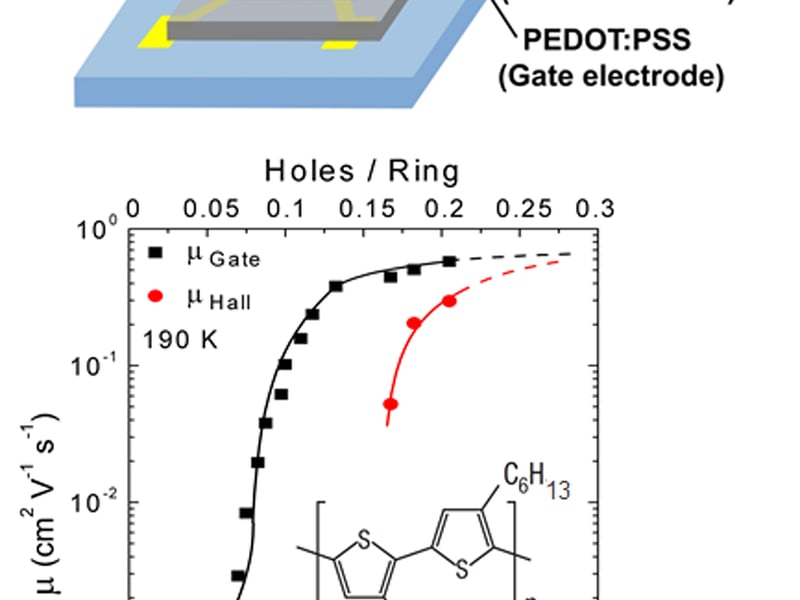
First Observation of Hall Effect in Polymer Transistors
C. Daniel Frisbie (IRG-2) & Chris Leighton (IRG-3)
Printed transistors employing both the bench-mark polymer semiconductor poly(3-hexyl-thiophene) and ultra-high capacitance ion gel gate insulators exhibit unusually large hole mobilities near 1 cm2/Vs at high charge densities (0.2 holes/ring).
Jan 16, 2013
University of Washington
SAPs: Self Assembled Peptides
Developed in GEMSEC, biocombinatorially selected solid binding peptides with short (7-15) amino acid (AA) sequences can bind to atomically flat materials via molecular recognition that leads to surface diffusion, clustering and long-range ordered assembly commensurate with the underlying crystallographic solid lattice.
Jan 16, 2013
University of Washington
Molecular Biomimetics
Molecular Biomimetics - Making materials one molecule at a time, via the Biology’s ways, allows an intricate control of nano- and microstructures that permit tailoring functional properties towards practical applications.

Jan 16, 2013
University of Minnesota - Twin Cities
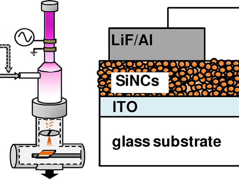
First All-Gas Phase Manufacture of a Nanocrystal Based Electronic Device
Uwe Kortshagen (IRG-4), Russell Holmes (IRG-2)
Semiconductor nanocrystals hold great potential for the low-cost manufacture of electronic devices.

Jan 16, 2013
University of Minnesota - Twin Cities
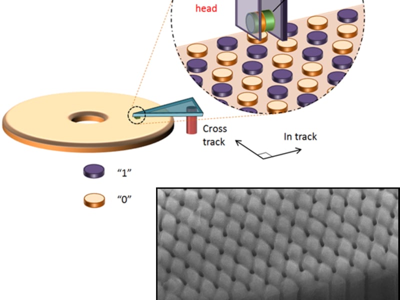
Low Resistivity Magnetic Nano-Sensors
Beth Stadler and Randy Victora (IRG-3)
As electronic devices shrink deep into the nano-scale, low-resistivities become essential.
Dec 18, 2012
University of Utah
MRSEC Takes the Lead in Coaching the Coaches in Materials Science Event
Utah MRSEC provided staff and faculty support for a Science Olympiad coaches’ clinic in November 2012, to help science teachers prepare to coach teams.
37 middle and high school science teachers, 22 of them female, from across the state dedicated their Saturday to attend the clinic to improve Science Olympiad team coaching skills.
Dec 4, 2012
Georgia Institute of Technology
Fabrication on Patterned Silicon Carbide Produces Bandgap for Graphene-Based Electronics
Ed Conrad, Lead Researcher, Georgia Institute of Technology
By fabricating graphene structures atop nanometer-scale “steps” etched into silicon carbide, researchers have for the first time created a substantial electronic bandgap in the material suitable for room-temperature electronics. Use of nanoscale topography to control the properties of graphene could facilitate fabrication of transistors and other devices, potentially opening the door for developing all-carbon integrated circuits.
Nov 28, 2012
Pennsylvania State University
Hidden Roto Symmetries in Nature Discovered
Venkatraman Gopalan (Penn State) and Daniel B. Litvin (Penn State)
MRSEC researchers have discovered a missing spatial operation in nature called rotation-reversal symmetry that reverses the sense of all static rotations in a crystal. Certain minerals, organic crystals or metamaterials are composed of subunits that can exist in two states: clockwise or counter-clockwise rotated. The symmetry of a crystal lattice helps determine the material’s properties, and certain properties can only exist in lattices with special symmetries. In perovskite complex oxides, for example, oxygen cages counter-rotate (see image); these crystals have twice as many
Showing 841 to 850 of 1398