
Highlights

Encapsulating 2D materials with boron nitride narrows emission linewidths, which is useful for integration into photonic devices.
Jun 5, 2018
Northwestern University

Encapsulated 2D Heterostructures for Enhanced Layered Optoelectronics

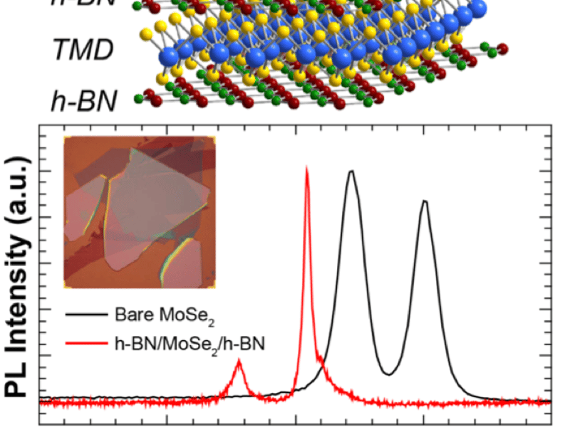
Two-dimensional (2D) layered materials have many features suitable for optoelectronic devices, but poor quality substrates can degrade optical properties. By encapsulating a monolayer semiconductor in layers of atomically-thin hexagonal boron nitride, a nearly pristine environment can be achieved free from surface roughness and defects of typical substrates.
Examples of the wide range of 3D microstructures that can be realized by controlled mechanical buckling of patterned two-dimensional materials.
Jun 5, 2018
Northwestern University

Controlled Mechanical Buckling for Origami-Inspired 3D Microstructures

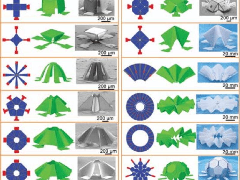
A new strategy has been introduced to exploit mechanical buckling for autonomic origami assembly of three-dimensional (3D) microstructures across a wide range of material classes, including soft polymers and brittle inorganic semiconductors, and length scales from nanometers to centimeters. The engineered folding creases are created through spatial variation of thickness in the initial two-dimensional structures.
(Left) Scanning electron microscopy images of DNA-linked gold nanodisk stacks. (Right) Optical extinction spectra of the stacks.
Jun 5, 2018
Northwestern University

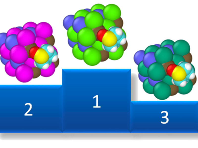
Tuning Optical Properties with DNA-Linked Gold Nanodisk Stacks

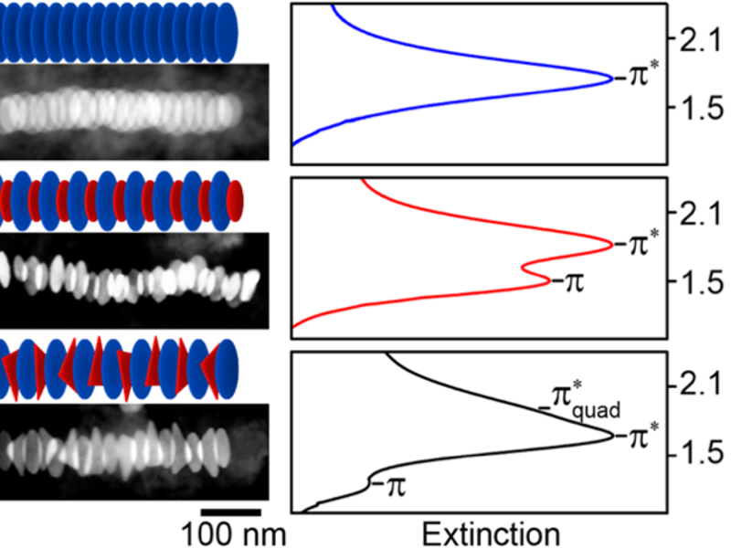
Recent advances in gold nanoparticle synthesis combined with functionalization with DNA linkers has enabled the self-assembly of stacks of gold nanodisks in which the optical spectra can be tuned and modulated by controlling the stack structure (e.g., particle spacing, arrangement, and stack length). The figure shows three possible arrangements of the particles, and the corresponding spectra that are associated with the plasmon resonance excitation in the stack.
Schematic of the molecular structure and vibrational modes of the perylene diimide molecules used in this study.
Jun 5, 2018
Northwestern University

Probing Intermolecular Interactions with Intramolecular Resolution

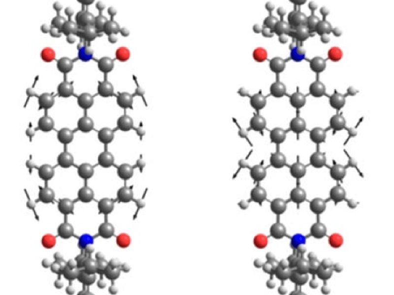
At the nanometer-scale, the surface area to volume ratio increases substantially compared to bulk materials. Consequently, methods for functionalizing and passivating surfaces can play a dominant role in determining the properties of nanomaterials. Of particular interest are self-assembled monolayers of organic molecules that have been widely used to control the electronic, optical, chemical, and frictional properties of nanomaterials in a range of applications.
(a) Thin-film transistor structures. (b) Mobility as a function of PEI concentration. (c) Schematic energy band diagram illustrating the shift of the In2O3 work function with PEI.
Jun 5, 2018
Northwestern University

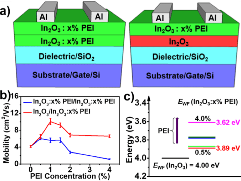
High Performance Heterojunction Oxide Thin Film Transistors

Due to their outstanding electronic properties and high optical transparency, metal oxide thin-film transistors have significant potential in state-of-the-art flat panel display technologies. Here, high performance solution-processed metal oxide thin-film transistors were realized by fabricating heterojunctions of indium oxide (In2O3) and polyethylenimine (PEI) as the semiconducting channel layer. Due to the tunable work function of the In2O3-PEI blends, electron mobilities as high as ~10 cm2V-1s-1 were obtained.
Synchrotron X-ray diffraction allows the evolution of the atomic structure of oxide films to be measured during crystallization.
Jun 5, 2018
Northwestern University

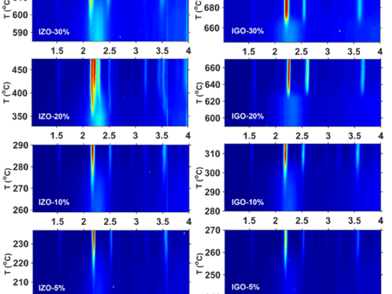
Amorphous to Crystalline Transition in Indium Oxide Semiconductors

Amorphous oxide semiconductors commonly are indium oxides doped with other metal ions. Although it is known that the introduction of secondary metal ions decreases the degree of crystallinity and elevates the crystallization temperature, there is a lack of systematic study to compare and quantify the effects of different dopant elements. In an interdisciplinary study within IRG-2 of the Northwestern University MRSEC, in situ synchrotron X-ray characterization was performed to characterize the isochronal crystallization process of oxide thin films synthesized by pulsed laser deposition.
X-ray standing wave characterization resolves the atomic structure of the synthetic 2D material borophene.
Jun 5, 2018
Northwestern University

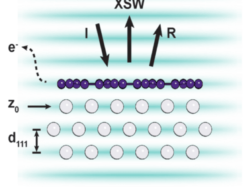
Atomic-Scale Characterization of Synthetic Two-Dimensional Materials

Atomically thin two-dimensional (2D) materials exhibit superlative properties dictated by their intralayer atomic structure, which is typically derived from a limited number of thermodynamically stable bulk layered crystals (e.g., graphene from graphite). The growth of entirely synthetic 2D crystals – those with no corresponding bulk allotrope – would circumvent this dependence upon bulk thermodynamics and substantially expand the phase space available for structure-property engineering of 2D materials.
Design of the two self-assembled molecular dielectrics used in this study. The orientation of the molecular dipole is inverted between the two cases, allowing control over dielectric polarization.
Jun 5, 2018
Northwestern University

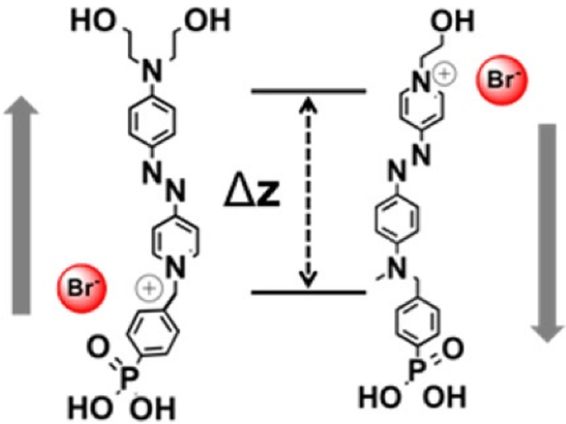
Controlling Dielectric Polarization via Molecular Design

Dielectric materials play a critical role in determining the operating voltage in modern-day electronics. In particular, highly polarizable and ultrathin dielectrics enable low operating voltages and thus low power consumption.
Schematic of atomically-thin superlattices where two different transition-metal dichalcogenide monolayers are “seamlessly stitched together” without dislocations at the interfaces.
S. Xie et al., Science 359, p. 1131-1136 (2018)
Schematic of atomically-thin superlattices where two different transition-metal dichalcogenide monolayers are “seamlessly stitched together” without dislocations at the interfaces. S. Xie et al., Science 359, p. 1131-1136 (2018)
Jun 5, 2018
Cornell University

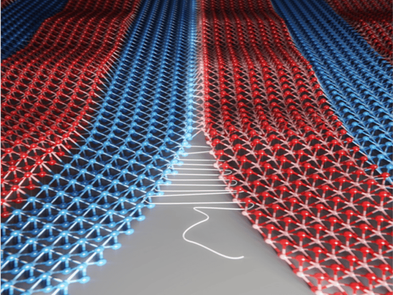
Three-Atom Thick Fabrics Made by Seamless Stitching of Single-Layer Crystals

Joining different materials can lead to all kinds of breakthroughs. In electronics, this produces heterojunctions — the most fundamental components in solar cells and computer chips. The smoother the seam between two materials, the better the electronic devices will function.
Accelerated searches, made possible by machine learning techniques, are of growing interest in materials discovery. A suitable case involves the solution processing of components that ultimately form thin films of solar cell materials known as Hybrid Organic-Inorganic Perovskites (HOIPs). The number of molecular species that combine in solution to form these films constitutes an overwhelmingly large “compositional" space (at times, exceeding 500,000 possible combinations). Selecting a HOIP with desirable characteristics involves choosing different cations, halides, and solvent blends from a diverse palette of options. An unguided search by experimental investigations or molecular simulations is prohibitively expensive. In this work, we propose a novel Bayesian optimization method that overcomes challenges where data is scarce, and in which the search space is given by binary variables indicating whether a constituent is present or not. We demonstrate that the proposed approach identifies HOIPs with the targeted maximum intermolecular binding energy between HOIP salt and solvent at considerably lower cost than previous state-of-the-art Bayesian optimization methodology and at a fraction of the time (less than 10 per cent) needed to complete an exhaustive search. We find an optimal composition within 15 iterations (plus or minus 10) in a HOIP compositional space containing 72 combinations, and within 29 iterations (plus or minus 11) when considering mixed halides (240 combinations). Exhaustive quantum mechanical simulations of all possible combinations were used to validate the optimal prediction from a Bayesian optimization approach. These proofs of concept demonstrate the undeniable promise of the novel Bayesian optimization methodology, presented here, to the field of materials discovery.
H. Herbol et al., Nature Comp. Materials, under review (2018)
Accelerated searches, made possible by machine learning techniques, are of growing interest in materials discovery. A suitable case involves the solution processing of components that ultimately form thin films of solar cell materials known as Hybrid Organic-Inorganic Perovskites (HOIPs). The number of molecular species that combine in solution to form these films constitutes an overwhelmingly large “compositional" space (at times, exceeding 500,000 possible combinations). Selecting a HOIP with desirable characteristics involves choosing different cations, halides, and solvent blends from a diverse palette of options. An unguided search by experimental investigations or molecular simulations is prohibitively expensive. In this work, we propose a novel Bayesian optimization method that overcomes challenges where data is scarce, and in which the search space is given by binary variables indicating whether a constituent is present or not. We demonstrate that the proposed approach identifies HOIPs with the targeted maximum intermolecular binding energy between HOIP salt and solvent at considerably lower cost than previous state-of-the-art Bayesian optimization methodology and at a fraction of the time (less than 10 per cent) needed to complete an exhaustive search. We find an optimal composition within 15 iterations (plus or minus 10) in a HOIP compositional space containing 72 combinations, and within 29 iterations (plus or minus 11) when considering mixed halides (240 combinations). Exhaustive quantum mechanical simulations of all possible combinations were used to validate the optimal prediction from a Bayesian optimization approach. These proofs of concept demonstrate the undeniable promise of the novel Bayesian optimization methodology, presented here, to the field of materials discovery. H. Herbol et al., Nature Comp. Materials, under review (2018)
Jun 5, 2018
Cornell University

Using Math to Search for a 'Needle in a Haystack' to Make Better Solar Cells

CCMR researchers have used mathematical methods, typically used in business forecasting, to suggest which combination of components will make the best solar cell materials in a “perovskite” arrangement. These materials are made in solution, essentially in a beaker, at room temperature. This makes them far more energy-conservative than traditional silicon solar cells. But researchers are spoiled for choice in terms of components that could be put into the “soup;” too many to make in the lab.