Highlights
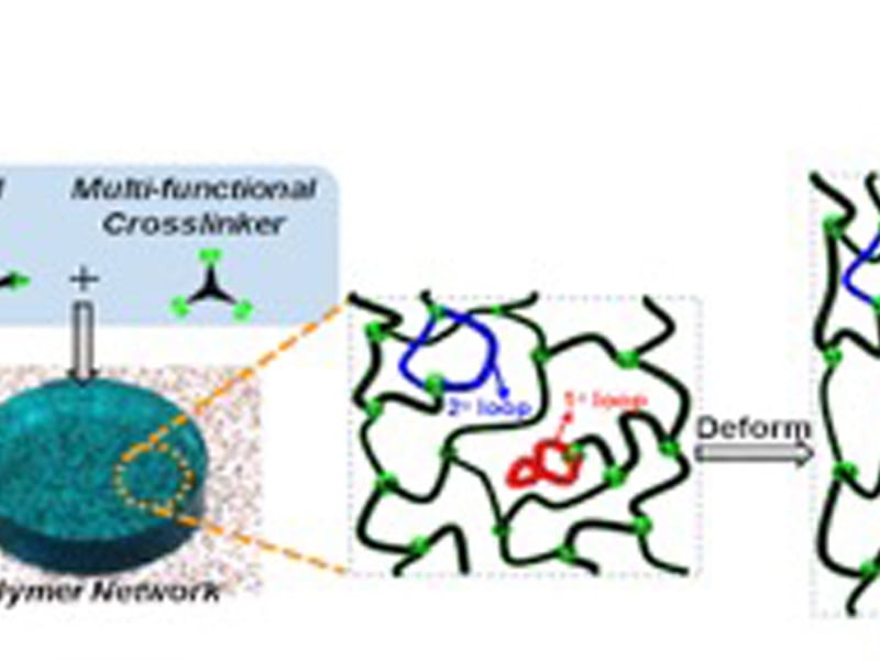
Understanding Loops in Polymer Networks Results in an Improved Theory for Rubbery Materials
Jeremiah Johnson
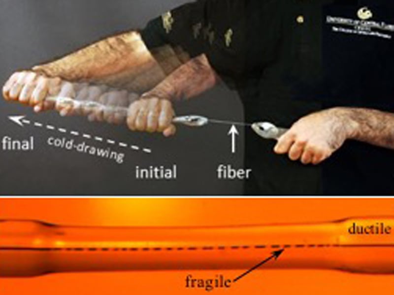
Controlled Fragmentation of Multimaterial Fibers Via Polymer Cold-Drawing
Ayman Abouraddy and Yoel Fink
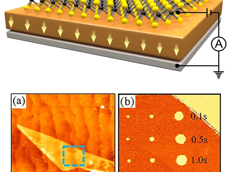
Hybrid 2D-Ferroelectric Structures for Information Technology
Alexei Gruverman, Alexander Sinitskii, and Evgeny Tsymbal (University of Nebraska-Lincoln) and Chang-Beom Eom (University of Wisconsin-Madison)
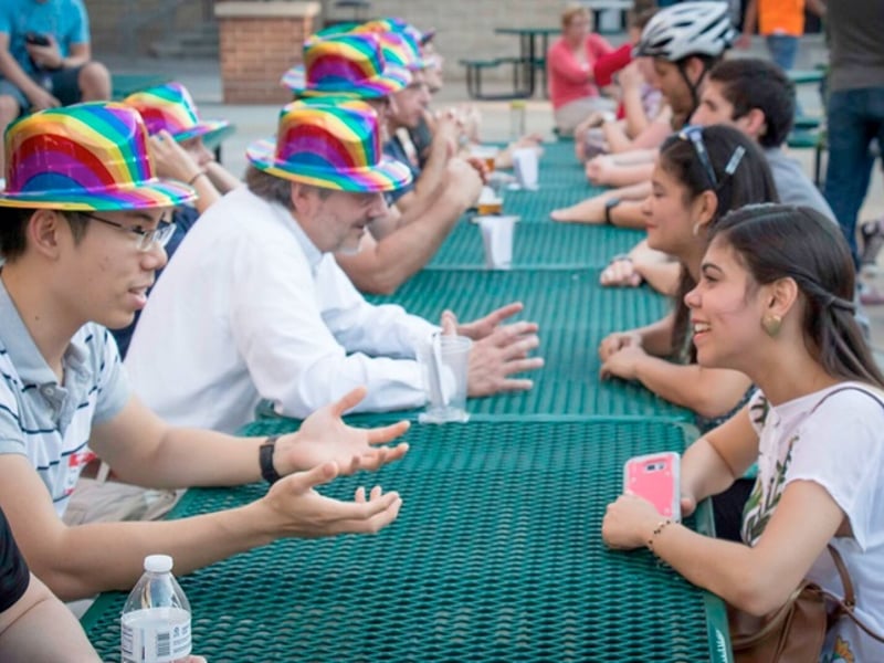
Science Night Live! : Bringing Science to the Public
Rebecca Lai and Jocelyn Bosley (Nebraska MRSEC)
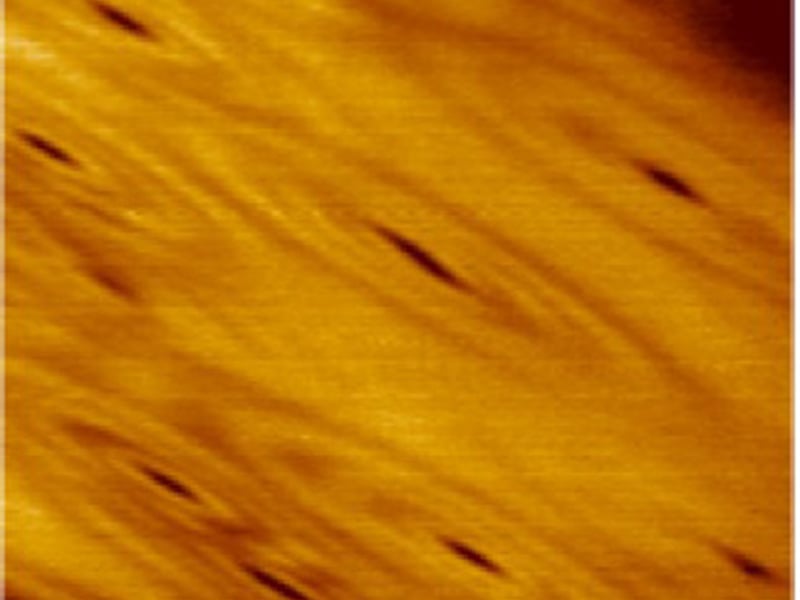
Real-Space Imaging of a Nematic Quantum Liquid
B. E. Feldman1, M. T. Randeria1, A. Gyenis1, F. Wu2, H. Ji1, R. J. Cava1, A. H. MacDonald2, A. Yazdani1 1Princeton University 2University of Texas at Austin
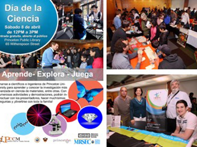
Princeton MRSEC: Dia De la Ciencia/Science Day
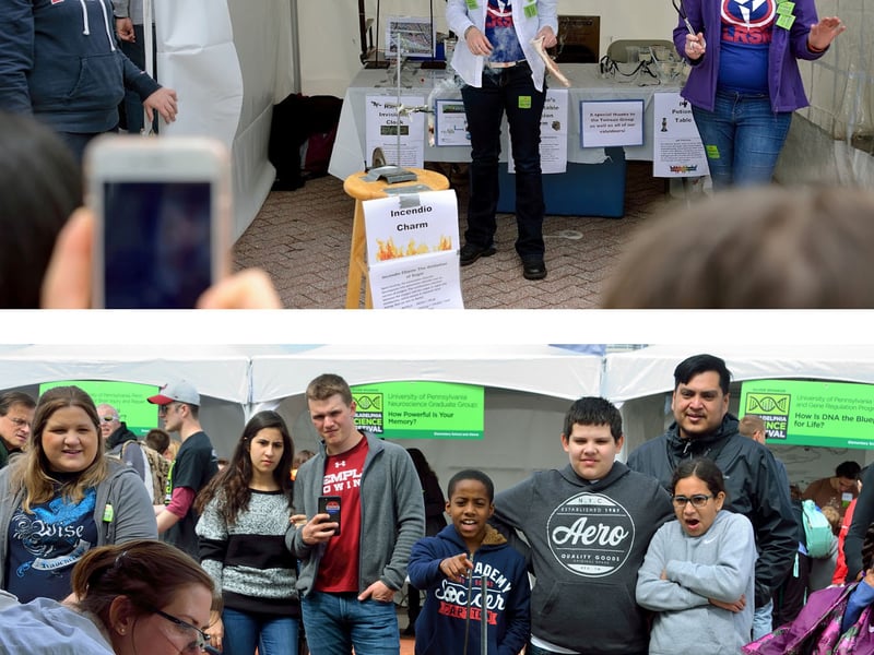
Philadelphia Science Festival
Zahra Fakhraai (Chemistry), Andrew R. McGhie (LRSM EDU) & Mark Licurse (LRSM EDU)
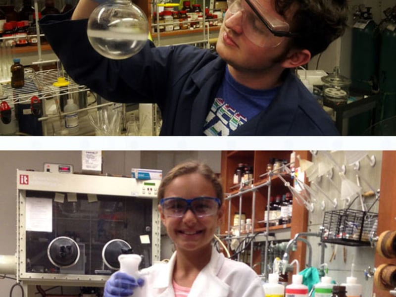
MRSEC-Related Research by High School Students
V. Percec (Chemistry), M. Kozlowski (Chemistry), D. Durian (Physics), A.R. McGhie (LRSM EDU) & M.W. Licurse (LRSM EDU)
Intellectual Merit: Long correlation length for glassy dynamics
Zahra Fakhraai (Chemistry), Karen Winey (Materials Science & Engineering), and Robert Riggleman (Chemical and Biomolecular Engineering) Graduate student Sarah Wolf demonstrates optical cloaking to Philadelphia high-school students at an event organized by the National Society of Black Engineers.
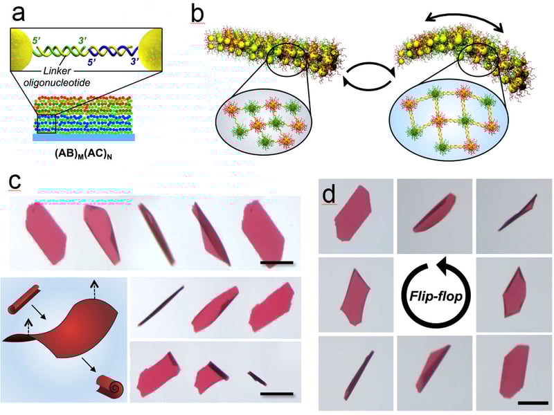
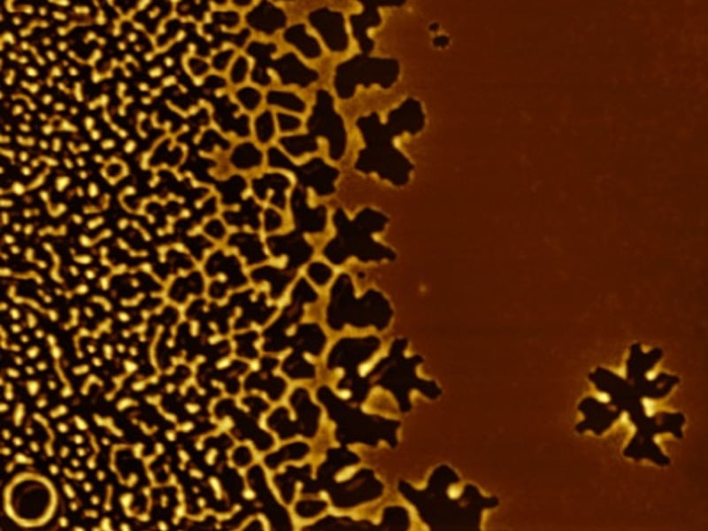
SEED Team Builds Simple Microrobots from DNA
T.S. Shim, D. Chenoweth (Chemistry), D. Lee (Chemical and Biomolecular Engineering), S.J. Park (Chemistry), J.C. Crocker (Chemical and Biomolecular Engineering) Dr. Tae Soup Shim (left) & Dr. Mehdi Zanjani (right)
Showing 551 to 560 of 1451