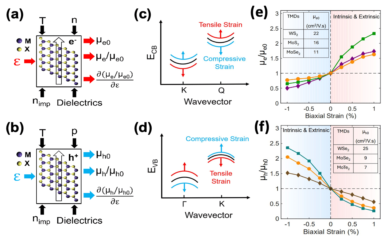
Two-dimensional (2D) materials like MoS2 and WSe2 are on semiconductor industry roadmaps to replace silicon in transistors in the next 10 years. A key challenge to realizing this vision is to understand the mechanisms limiting how electrons move through these materials, called the mobility, and how to manipulate the mobility to maximize the performance of devices.
The Illinois MRSEC has developed new multiscale simulations to capture all major sources of scattering that slow down charge flow, and has carefully validated the models with experimental data. They discovered that the major limiting mechanism of mobility rises from intervalley scattering. They found that modulating strain tunes the intervalley scattering by changing the relative energies of different conduction valleys, leading to a dramatic increase in mobility. For example, stretching MoS2 increases electron mobility in n-type transistors by about 1.7 times per 1% strain, while compressing WSe2 boosts hole mobility in p-type transistors by about 2.3 times per 1%. These gains are much larger than in silicon and remain effective across many different real-world conditions, making strain a dependable method for improving future computer chips that is multiplicative with other strategies like defect control.
This achievement supports Illinois MRSEC IRG1 by leveraging strain in 2D materials to precisely control charge flow, and guide industry in advancing the goal of designing efficient, faster nanoscale electronic devices.
Strain-tunable inter-valley scattering defines universal mobility enhancement in n- and p-type 2D TMDs
Illinois Materials Research Science and Engineering Center
I-MRSEC has a mission to perform fundamental, innovative research that supports technological applications in areas of societal need, while promoting interdisciplinary materials-focused education and training of students.