In nanoscale devices, we have the opportunity to isolate the individual physical processes of noise.Â’ Â’ Time-resolved STM imaging of fluctuating nanoscale structure shows that the motion of surface line boundaries (steps) is coupled 10x more strongly to scattering of electrical carriers than predicted from zero-temperature calculations.Â’ The resulting changes in surface resistivity will carry the spectral characteristic of the step fluctuations, yielding a distinct noise signature SI ~ f-3/4.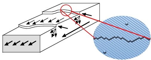
Scattering at Nanoscale Structure in Metals
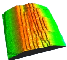
Top above: Scanning Tunneling Microscope (STM) image of the top of a 20 nm diameter crystalline Ag wire. The longitudinal structures are steps - changes in height by a single atomic layer.
Middle above: Schematic illustration of the scattering of charge carriers at surface steps, with expanded image illustrating the thermal excitations of the atomic structure that cause step motion.
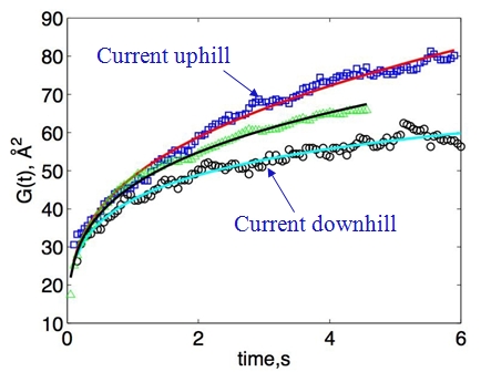
Bottom left: The thermal motion of the steps, shown by the correlation function G(t), is enhanced or suppressed when current flows uphill or downhill with respect to the step direction.
UMD Materials Research Science and Engineering Center (2005)
The Maryland MRSEC carries out nationally recognized fundamental research on surfaces and interfaces of materials with potential impact on the next generation of opto- and nano-electronic devices, and on complex oxides with potential applications in memory, switches, and sensors.