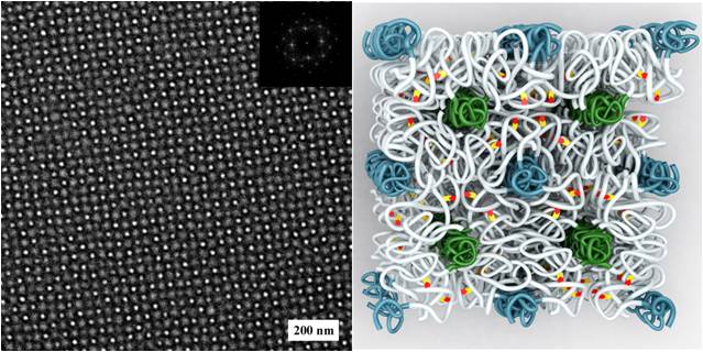
The manufacture of smaller, faster and more efficient microelectronic components is a major scientific and technological challenge, driven in part by a constant need for smaller lithographically defined features and patterns. While traditional self-assembling approaches based on block copolymer lithography spontaneously form nanometer sized hexagonal structures, these features are not consistent with the industry standard square coordinate system. As reported in the popular press and Science, combining supramolecular assembly of hydrogen-bonding units with controlled phase separation of diblock copolymers, now has been shown to give nanoscale square patterns. A major boost to the US semiconductor industry.
Materials Research Science and Engineering Center at UCSB
The NSF Materials Research Science and Engineering Center at UC Santa Barbara develops and sustains a productive, collaborative, and engaged community that drives a portfolio of transformative materials research and empowers a diverse workforce.