Background: Most
organic devices, from organic light emitting diodes to organic
spintronic devices vertical devices, where the essential interfaces are
buried and thus not subject to investigation.
This work: Using a novel fabrication method to
fabricate lateral devices,as schematically shown in Fig.1. The lateral
geometry allows the application of a transverse field through the gate
terminal at the back of the substrate, allowing the surface potentials
at the junction to be probed directly using Scanning Kelvin probe
microscopy (SKPM) while the device is in
operation.
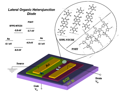
Fig.1: Schematics of a lateral device, also showing the molecular structures and their energy levels.
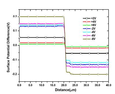
Fig. 2: Variation of built-in potential with applied lateral voltage (forward and reverse) and gate terminal grounded.