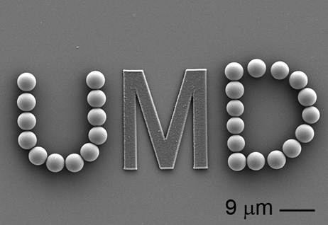
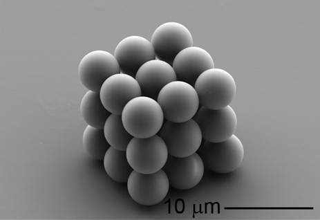
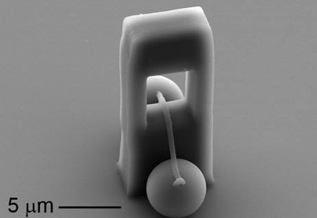
Realizing the full potential of nanodevices will require the ability to place individual elements that are much smaller than the width of a human hair in precise, 3-D configurations. We have developed new materials that allow us to use light and/or electric fields to position individual micro- or nanostructures in precise locations in three dimensions and then to lock them into place using short pulses of light from a laser. This “trap-and-zap” scheme is being used to create new types of optical, electronic and mechanical devices based on nanotechnology. Shown here are 2D pattern (top), a 3D cube (middle), and a “needle and thread” (bottom) created with this technique.


UMD Materials Research Science and Engineering Center (2005)
The Maryland MRSEC carries out nationally recognized fundamental research on surfaces and interfaces of materials with potential impact on the next generation of opto- and nano-electronic devices, and on complex oxides with potential applications in memory, switches, and sensors.