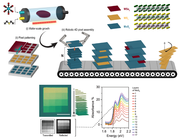
 As new methods are established to synthesize atomically-thin quantum materials, it becomes necessary to develop a technique to take those materials and assemble them into complex structures. Chicago and Cornell researchers have demonstrated an automated robotic technique that takes (i, right) wafer-scale grown materials that are (ii) precisely patterned into “pixel”-like building blocks and (iii) assembles them into deliberate geometries. Structures with at least 80 layers can be assembled at a rate of 30 layers per hour.
This technique could accelerate discovery of new functional materials as it allows for rapid study of permutations of stacked materials. One example is using these structures to examine the absorption or emission of light as a function of different thicknesses and material ordering, all within a single structure (bottom right). Another example is to study the effects of twisted stacking of the layers on electrical properties.
In the future, the technique may be used to assemble electronic or optical devices.